P R E L I M I N A R Y
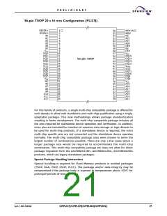
Pin Description
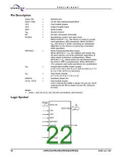
Amax–A0
DQ15–DQ0
CE#
OE#
WE#
VSS
NC
RY/BY#
=
=
=
=
=
=
=
=
Address bus
16-bit data inputs/outputs/float
Chip Enable Inputs
Output Enable Input
Write Enable
Device Ground
Pin Not Connected Internally
Ready/Busy output and open drain.
When RY/BY#= VIH, the device is ready to accept
read operations and commands. When RY/BY#=
VOL, the device is either executing an embedded
algorithm or the device is executing a hardware
reset operation.
WP#/ACC
=
Write Protect/Acceleration Input.
When WP#/ACC= VIL, the highest and lowest two
4K-word sectors are write protected regardless of
other sector protection configurations. When
WP#/ACC= VIH, these sector are unprotected unless
the DYB or PPB is programmed. When WP#/ACC=
12V, program and erase operations are accelerated.
VIO
=
=
Input/Output Buffer Power Supply
(1.65 V to 1.95 V (for PL127J and PL129J) or 2.7 V
to 3.6 V (for all PLxxxJ devices))
Chip Power Supply
VCC
(2.7 V to 3.6 V or 2.7 to 3.3 V)
RESET#
CE1#, CE2#
=
=
Hardware Reset Pin
Chip Enable Inputs.
CE1# controls the 64Mb in Banks 1A and 1B. CE2#
controls the 64 Mb in Banks 2A and 2B. (Only for
PL129J)
Notes:
1. Amax = A22 (PL127J), A21 (PL129J and PL064J), A20 (PL032J)
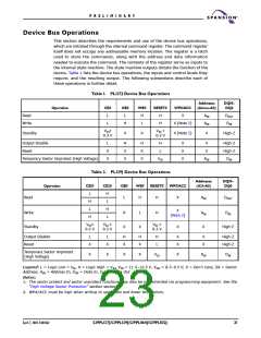
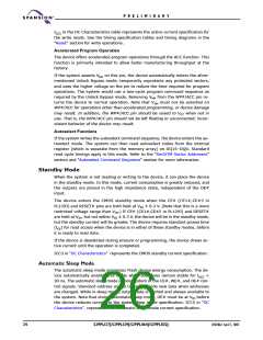
Logic Symbol
max+1
Amax–A0
16
DQ15–DQ0
CE#
OE#
WE#
WP#/ACC
RESET#
RY/BY#
VIO (VCCQ
)
20
S29PL127J/S29PL129J/S29PL064J/S29PL032J
31107A62 April 7, 2005

 SPANSION [ SPANSION ]