A d v a n c e I n f o r m a t i o n
Write Operation Status
The device provides several bits to determine the status of a write operation:
DQ2, DQ3, DQ5, DQ6, DQ7, and RY/BY#. Table 21 and the following subsections
describe the functions of these bits. DQ7, RY/BY#, and DQ6 each offer a method
for determining whether a program or erase operation is complete or in progress.
These three bits are discussed first.
DQ7: Data# Polling
The device features a Data# polling flag as a method to indicate to the host sys-
tem whether the embedded algorithms are in progress or are complete. During
the Embedded Program Algorithm an attempt to read the bank in which program-
ming was initiated will produce the complement of the data last written to DQ7.
Upon completion of the Embedded Program Algorithm, an attempt to read the de-
vice will produce the true last data written to DQ7. Note that DATA# polling
returns invalid data for the address being programmed or erased.
For example, the data read for an address programmed as 0000 0000 1000
0000b will return XXXX XXXX 0XXX XXXXb during an Embedded Program opera-
tion. Once the Embedded Program Algorithm is complete, the true data is read
back on DQ7. Note that at the instant when DQ7 switches to true data, the other
bits may not yet be true. However, they will all be true data on the next read from
the device. Please note that Data# polling may give misleading status when an
attempt is made to write to a protected sector.
For chip erase, the Data# polling flag is valid after the rising edge of the sixth
WE# pulse in the six write pulse sequence. For sector erase, the Data# polling is
valid after the last rising edge of the sector erase WE# pulse. Data# polling must
be performed at sector addresses within any of the sectors being erased and not
a sector that is a protected sector. Otherwise, the status may not be valid. DQ7
= 0 during an Embedded Erase Algorithm (chip erase or sector erase operation)
but will return a “1” after the operation completes because it will have dropped
back into read mode.
In asynchronous mode, just prior to the completion of the Embedded Algorithm
operations, DQ7 may change asynchronously while OE# is asserted low. (In syn-
chronous mode, ADV# exhibits this behavior.) The status information may be
invalid during the instance of transition from status information to array (mem-
ory) data. An extra validity check is therefore specified in the data polling
algorithm. The valid array data on DQ31–DQ0 is available for reading on the next
successive read attempt.
The Data# polling feature is only active during the Embedded Programming Al-
gorithm, Embedded Erase Algorithm, Erase Suspend, Erase Suspend-Program
mode, or sector erase time-out.
If the user attempts to write to a protected sector, Data# polling will be activated
for about 1 µs: the device will then return to read mode, with the data from the
protected sector unchanged. If the user attempts to erase a protected sector,
Toggle Bit (DQ6) will be activated for about 150 µs; the device will then return to
read mode, without having erased the protected sector.
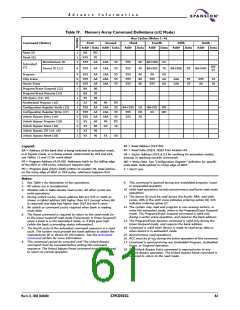
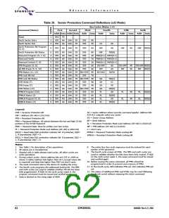
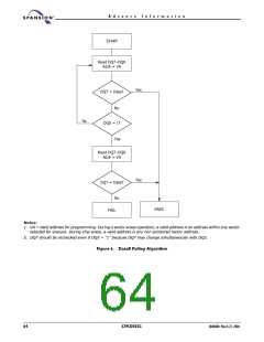
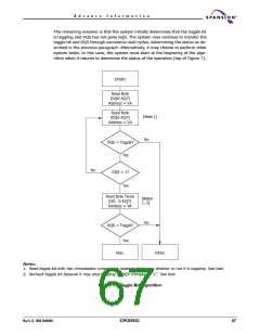
Table 21 shows the outputs for Data# Polling on DQ7. Figure 6 shows the Data#
Polling algorithm. Figure 24 shows the timing diagram for synchronous status
DQ7 data polling.
March 22, 2004 30606B0
S29CD032G
63

 SPANSION [ SPANSION ]