A d v a n c e I n f o r m a t i o n
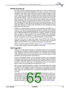
Table 19. Memory Array Command Definitions (x32 Mode)
Bus Cycles (Notes 1–4)
Command (Notes)
First
Second
Third
Fourth
Fifth
Addr
Sixth
Addr
Addr Data Addr Data
Addr
Data
Addr
Data
Data
Data
Read (5)
Reset (6)
1
1
4
RA
RD
F0
XXX
555
Manufacturer ID
Device ID (11)
AA
2AA
2AA
55
55
555
555
90
90
BA+X00
BA+X01
01
7E
Autoselect
(7)
00/
01
6
555
AA
BA+X0E
09
BA+X0F
Program
4
6
6
1
1
1
2
3
4
3
2
2
1
2
555
555
555
BA
AA
AA
AA
B0
30
98
A0
AA
AA
AA
A0
80
98
90
2AA
2AA
2AA
55
55
55
555
555
555
A0
80
80
PA
PD
AA
AA
Chip Erase
Sector Erase
555
555
2AA
2AA
55
55
555
SA
10
30
Program/Erase Suspend (12)
Program/Erase Resume (13)
CFI Query (14, 15)
BA
55
Accelerated Program (16)
Configuration Register Verify (15)
Configuration Register Write (17)
Unlock Bypass Entry (18)
Unlock Bypass Program (18)
Unlock Bypass Erase (18)
Unlock Bypass CFI (14, 18)
Unlock Bypass Reset (18)
XX
PA
2AA
2AA
2AA
PA
PD
55
55
55
PD
10
555
555
555
XX
BA+555
555
C6
D0
20
BA+XX
XX
RD
WD
555
XX
XX
XX
XX
XX
00
RA = Read Address (A19:A0).
RD = Read Data (DQ31:DQ0) from location RA.
Legend:
BA = Address of the bank that is being switched to autoselect mode,
is in bypass mode, or is being erased. Determined by A19 and A18,
see Tables 11 and 12 for more detail.
SA = Sector Address (A19:A11) for verifying (in autoselect mode),
erasing, or applying security commands.
PA = Program Address (A19:A0). Addresses latch on the falling edge
of the WE# or CE# pulse, whichever happens later.
WD = Write Data. See “Configuration Register” definition for specific
write data. Data latched on rising edge of WE#.
PD = Program Data (DQ31:DQ0) written to location PA. Data latches
on the rising edge of WE# or CE# pulse, whichever happens first.
X = Don’t care
Notes:
1. See Table 1 for description of bus operations.
2. All values are in hexadecimal.
3. Shaded cells in table denote read cycles. All other cycles are
write operations.
9. This command is ignored during any embedded program, erase
or suspended operation.
10. Valid read operations include asynchronous and burst read mode
operations.
11. The device ID must be read across the fourth, fifth, and sixth
cycles. 00h in the sixth cycle indicates ordering option 00, 01h
indicates ordering option 01.
12. The system may read and program in non-erasing sectors, or
enter the autoselect mode, when in the Program/Erase Suspend
mode. The Program/Erase Suspend command is valid only
during a sector erase operation, and requires the bank address.
13. The Program/Erase Resume command is valid only during the
Erase Suspend mode, and requires the bank address.
14. Command is valid when device is ready to read array data or
when device is in autoselect mode.
4. During unlock cycles, (lower address bits are 555 or 2AAh as
shown in table) address bits higher than A11 (except where BA
is required) and data bits higher than DQ7 are don’t cares.
5. No unlock or command cycles required when bank is reading
array data.
6. The Reset command is required to return to the read mode (or
to the erase-suspend-read mode if previously in Erase Suspend)
when a bank is in the autoselect mode, or if DQ5 goes high
(while the bank is providing status information).
7. The fourth cycle of the autoselect command sequence is a read
cycle. The system must provide the bank address to obtain the
manufacturer ID or device ID information. See the Autoselect
Command section for more information.
15. Asynchronous read operations.
16. ACC must be at V during the entire operation of this command.
ID
8. This command cannot be executed until The Unlock Bypass
command must be executed before writing this command
sequence. The Unlock Bypass Reset command must be executed
to return to normal operation.
17. Command is ignored during any Embedded Program, Embedded
Erase, or Suspend operation.
18. The Unlock Bypass Entry command is required prior to any
Unlock Bypass operation. The Unlock Bypass Reset command is
required to return to the read mode.
March 22, 2004 30606B0
S29CD032G
61

 SPANSION [ SPANSION ]