A d v a n c e I n f o r m a t i o n
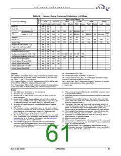
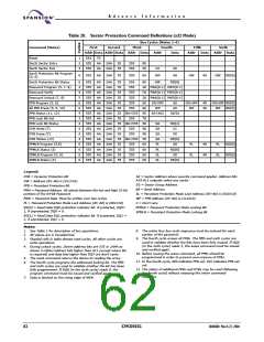
Table 20. Sector Protection Command Definitions (x32 Mode)
Bus Cycles (Notes 1-4)
Command (Notes)
First
Second
Third
Fourth
Fifth
Sixth
Addr Data Addr Data
Addr
Data
Addr
Data
Addr
Data
Addr
Data
Reset
1
3
4
XXX
555
555
F0
AA
AA
SecSi Sector Entry
SecSi Sector Exit
2AA
2AA
55
55
555
555
88
90
XX
OW
OW
00
68
SecSi Protection Bit Program
(5, 6)
6
555
AA
2AA
55
555
60
60
OW
48
OW
RD(0)
SecSi Protection Bit Status
Password Program (5, 7, 8)
Password Verify
6
4
4
5
6
6
4
3
4
4
4
4
6
6
6
6
555
555
555
555
555
555
555
555
555
555
555
555
555
555
555
555
AA
AA
AA
AA
AA
AA
AA
AA
AA
AA
AA
AA
AA
AA
AA
AA
2AA
2AA
2AA
2AA
2AA
2AA
2AA
2AA
2AA
2AA
2AA
2AA
2AA
2AA
2AA
2AA
55
55
55
55
55
55
555
555
555
555
555
555
RD(0)
38 PWA[0-1] PWD[0-1]
C8 PWA[0-1] PWD[0-1]
28 PWA[0-1] PWD[0-1]
Password Unlock (7, 8)
PPB Program (5, 6)
All PPB Erase (5, 9, 10)
PPB Status (11, 12)
PPB Lock Bit Set
60
60
SG+WP
WP
68
60
SG+WP
WP
48
40
SG+WP RD(0)
WP
RD(0)
55 BA+555 90
55 555 78
55 BA+555 58
SA+X02
00/01
PPB Lock Bit Status
DYB Write (7)
SA
SA
SA
SA
PL
RD(1)
X1
55
55
555
555
48
48
DYB Erase (7)
X0
DYB Status (12)
55 BA+555 58
RD(0)
68
PPMLB Program (5,6)
PPMLB Status (5)
55
55
55
55
555
555
555
555
60
60
60
60
PL
SL
48
48
PL
SL
RD(0)
RD(0)
PL
RD(0)
68
SPMLB Program (5, 6)
SPMLB Status (5)
SL
SL
RD(0)
Legend:
DYB = Dynamic Protection Bit
OW = Address (A5–A0) is (011X10).
PPB = Persistent Protection Bit
SA = Sector Address where security command applies. Address bits
A19:A11 uniquely select any sector.
SG = Sector Group Address
BA = Bank Address
PWA = Password Address. A0 selects between the low and high 32-bit
portions of the 64-bit Password
SL = Persistent Protection Mode Lock Address (A5–A0) is (010X10)
WP = PPB Address (A5–A0) is (111010)
X = Don’t care
PWD = Password Data. Must be written over two cycles.
PL = Password Protection Mode Lock Address (A5–A0) is (001X10)
RD(0) = Read Data DQ0 protection indicator bit. If protected, DQ0=
1, if unprotected, DQ0 = 0.
PPMLB = Password Protection Mode Locking Bit
SPMLB = Persistent Protection Mode Locking Bit
RD(1) = Read Data DQ1 protection indicator bit. If protected, DQ1 =
1, if unprotected, DQ1 = 0.
Notes:
1. See Table 1 for description of bus operations.
2. All values are in hexadecimal.
8. The entire four bus-cycle sequence must be entered for each
portion of the password.
9. The fourth cycle erases all PPBs. The fifth and sixth cycles are
used to validate whether the bits have been fully erased. If DQ0
(in the sixth cycle) reads 1, the erase command must be issued
and verified again.
10. Before issuing the erase command, all PPBs should be
programmed in order to prevent over-erasure of PPBs.
3. Shaded cells in table denote read cycles. All other cycles are
write operations.
4. During unlock cycles, (lower address bits are 555 or 2AAh as
shown in table) address bits higher than A11 (except where BA
is required) and data bits higher than DQ7 are don’t cares.
5. The reset command returns the device to reading the array.
6. The fourth cycle programs the addressed locking bit. The fifth
and sixth cycles are used to validate whether the bit has been
fully programmed. If DQ0 (in the sixth cycle) reads 0, the
program command must be issued and verified again.
7. Data is latched on the rising edge of WE#.
11. In the fourth cycle, 00h indicates PPB set; 01h indicates PPB not
set.
12. The status of additional PPBs and DYBs may be read (following
the fourth cycle) without reissuing the entire command
sequence.
62
S29CD032G
30606B0 March 22, 2004

 SPANSION [ SPANSION ]