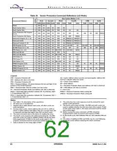
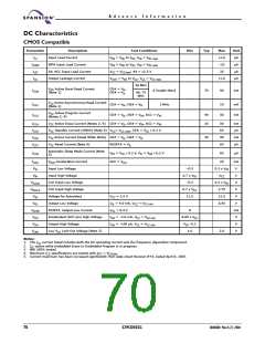
A d v a n c e I n f o r m a t i o n
If a program address falls within a protected sector, DQ6 toggles for approxi-
mately 1 µs after the program command sequence is written, then returns to
reading array data.
DQ6 also toggles during the erase-suspend-program mode, and stops toggling
once the Embedded Program algorithm is complete.
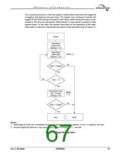
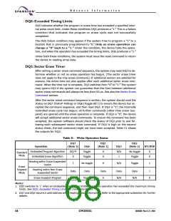
Table 21 shows the outputs for Toggle Bit I on DQ6. Figure 7 shows the toggle bit
algorithm in flowchart form, and the section Reading Toggle Bits DQ6/DQ2 ex-
plains the algorithm. Figure 25 in the AC Characteristics section shows the toggle
bit timing diagrams. Figure 25 shows the differences between DQ2 and DQ6 in
graphical form. See also the subsection on DQ2: Toggle Bit II. Figure 25 shows
the timing diagram for synchronous toggle bit status.
DQ2: Toggle Bit II
The “Toggle Bit II” on DQ2, when used with DQ6, indicates whether a particular
sector is actively erasing (that is, the Embedded Erase algorithm is in progress),
or whether that sector is erase-suspended. Toggle Bit II is valid after the rising
edge of the final WE# pulse in the command sequence.
DQ2 toggles when the system performs two immediately consecutive reads at
addresses within those sectors that have been selected for erasure. (For asyn-
chronous mode, either OE# or CE# can be used to control the read cycles. For
synchronous mode, ADV# is used.) But DQ2 cannot distinguish whether the sec-
tor is actively erasing or is erase-suspended. DQ6, by comparison, indicates
whether the device is actively erasing, or is in Erase Suspend, but cannot distin-
guish which sectors are selected for erasure. Thus, both status bits are required
for sector and mode information. Refer to Table 21 to compare outputs for DQ2
and DQ6.
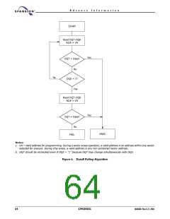
Figure 7 shows the toggle bit algorithm in flowchart form, and the section Reading
Toggle Bits DQ6/DQ2 explains the algorithm. See also the DQ6: Toggle Bit I sub-
section. 25 shows the toggle bit timing diagram. Figure 26 shows the differences
between DQ2 and DQ6 in graphical form. Figure 27 shows the timing diagram for
synchronous DQ2 toggle bit status.
Reading Toggle Bits DQ6/DQ2
Refer to 25 for the following discussion. Whenever the system initially begins
reading toggle bit status, it must perform two immediately consecutive reads of
DQ7–DQ0 to determine whether a toggle bit is toggling. Typically, the system
would note and store the value of the toggle bit after the first read. After the sec-
ond read, the system would compare the new value of the toggle bit with the first.
If the toggle bit is not toggling, the device has completed the program or erase
operation. The system can read array data on DQ7–DQ0 on the following read
cycle.
However, if after the initial two immediately consecutive read cycles, the system
determines that the toggle bit is still toggling, the system also should note
whether the value of DQ5 is high (see the section on DQ5). If it is, the system
should then determine again whether the toggle bit is toggling, since the toggle
bit may have stopped toggling just as DQ5 went high. If the toggle bit is no longer
toggling, the device has successfully completed the program or erase operation.
If it is still toggling, the device did not complete the operation successfully, and
the system must write the reset command to return to reading array data.
66
S29CD032G
30606B0 March 22, 2004

 SPANSION [ SPANSION ]