A d v a n c e I n f o r m a t i o n
cycle contains the program address and data. Additional data is programmed in
the same manner. This mode dispenses with the initial two unlock cycles required
in the standard program command sequence, resulting in faster total program-
ming time. Tables 18 and 20 show the requirements for the command sequence.
During the unlock bypass mode, only the Unlock Bypass Program and Unlock By-
pass Reset commands are valid. To exit the unlock bypass mode, the system
must issue the two-cycle unlock bypass reset command sequence. The first cycle
must contain the data 90h; the second cycle the data 00h. Addresses are don’t
care for both cycles. The device then returns to reading array data.
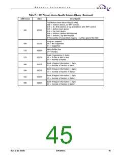
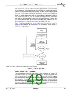
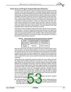
Figure 4 illustrates the algorithm for the program operation. See the Erase/Pro-
gram Operations table in AC Characteristics for parameters, and to Figures 21
and 22 for timing diagrams.
START
Write Program
Command Sequence
Data Poll
from System
Embedded
Program
algorithm
in progress
Verify Data?
No
Yes
No
Increment Address
Last Address?
Yes
Programming
Completed
Note: See Tables 19 and 20 for program command sequence.
Figure 4. Program Operation
Unlock Bypass Entry Command
The Unlock Bypass command, once issued, is used to bypass the “unlock” se-
quence for program, chip erase, and CFI commands. This feature permits slow
PROM programmers to significantly improve programming/erase throughput
since the command sequence often requires microseconds to execute a single
write operation. Therefore, once the Unlock Bypass command is issued, only the
two-cycle program and erase bypass commands are required. The Unlock Bypass
Command is ignored if the SecSi sector is enabled. To return back to normal op-
eration, the Unlock Bypass Reset Command must be issued.
March 22, 2004 30606B0
S29CD032G
49

 SPANSION [ SPANSION ]