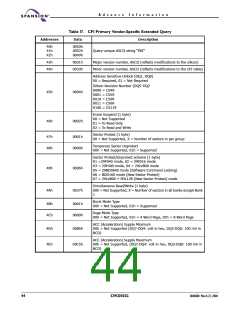
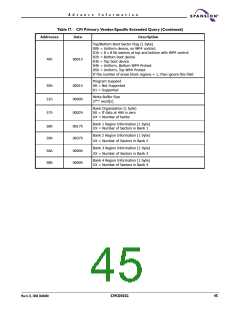
A d v a n c e I n f o r m a t i o n
mand. The program address and data are written next, which in turn initiate the
Embedded Program algorithm. The system is not required to provide further con-
trols or timings. The device automatically generates the program pulses and
verifies the programmed cell margin. Tables 19 and 20 show the address and
data requirements for the program command sequence.
During the Embedded Program algorithm, the system can determine the status
of the program operation by using DQ7, DQ6, or RY/BY#. (See Write Operation
Status for information on these status bits.) When the Embedded Program algo-
rithm is complete, the device returns to reading array data and addresses are no
longer latched. Note that an address change is required to begin read valid array
data.
Except for Program Suspend, any commands written to the device during the Em-
bedded Program Algorithm are ignored. Note that a hardware reset
immediately terminates the programming operation. The command sequence
should be reinitiated once that bank has returned to reading array data, to ensure
data integrity.
Programming is allowed in any sequence and across sector boundaries. A bit
cannot be programmed from a “0” back to a “1”. Attempting to do so may
halt the operation and set DQ5 to “1,” or cause the Data# Polling algorithm to
indicate the operation was successful. However, a succeeding read will show that
the data is still “0”. Only erase operations can convert a “0” to a “1”.
Accelerated Program Command
The Accelerated Chip Program mode is designed to improve the Word or Double
Word programming speed. Improving the programming speed is accomplished by
using the ACC pin to supply both the wordline voltage and the bitline current in-
stead of using the V pump and drain pump, which is limited to 2.5 mA. Because
PP
the external ACC pin is capable of supplying significantly large amounts of current
compared to the drain pump, all 32 bits are available for programming with a sin-
gle programming pulse. This is an enormous improvement over the standard 5-
bit programming. If the user is able to supply an external power supply and con-
nect it to the ACC pin, significant time savings are realized.
In order to enter the Accelerated Program mode, the ACC pin must first be taken
to V
(12 V ± 0.5 V) and followed by the one-cycle command with the program
HH
address and data to follow. The Accelerated Chip Program command is only exe-
cuted when the device is in Unlock Bypass mode and during normal read/reset
operating mode.
In this mode, the write protection function is bypassed unless the PPB Lock Bit =
1.
The Accelerated Program command is not permitted if the SecSi sector is
enabled.
Unlock Bypass Command Sequence
The unlock bypass feature allows the system to program words to the device
faster than using the standard program command sequence. The unlock bypass
command sequence is initiated by first writing two unlock cycles. This is followed
by a third write cycle containing the unlock bypass command, 20h. The device
then enters the unlock bypass mode. A two-cycle unlock bypass program com-
mand sequence is all that is required to program in this mode. The first cycle in
this sequence contains the unlock bypass program command, A0h; the second
48
S29CD032G
30606B0 March 22, 2004

 SPANSION [ SPANSION ]