A d v a n c e I n f o r m a t i o n
the programming operation. The command sequence should be reinitiated once
that bank has returned to reading array data, to ensure data integrity.
The Embedded Erase algorithm erase begins on the rising edge of the last WE#
or CE# pulse (whichever occurs first) in the command sequence. The status of
the erase operation is determined three ways:
Data# polling of the DQ7 pin (see DQ7: Data# Polling)
Checking the status of the toggle bit DQ6 (see DQ6: Toggle Bit I)
Checking the status of the RY/BY# pin (see RY/BY#: Ready/Busy#)
Once erasure has begun, only the Erase Suspend command is valid. All other
commands are ignored.
When the Embedded Erase algorithm is complete, the device returns to reading
array data, and addresses are no longer latched. Note that an address change is
required to begin read valid array data.
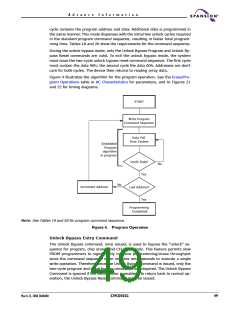
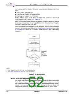
Figure 5 illustrates the Embedded Erase Algorithm. See the Erase/Program Oper-
ations tables in AC Characteristics for parameters, and to Figures 21 and 22 for
timing diagrams.
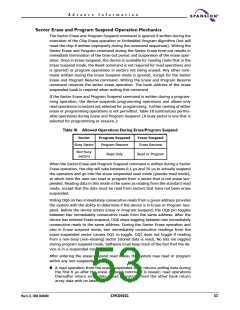
Sector Erase Command
The Sector Erase command is used to erase individual sectors or the entire flash
memory contents. Sector erase is a six-bus cycle operation. There are two “un-
lock” write cycles, followed by writing the erase “set up” command. Two more
“unlock” write cycles are then followed by the erase command (30h). The sector
address (any address location within the desired sector) is latched on the falling
edge of WE# or CE# (whichever occurs last) while the command (30h) is latched
on the rising edge of WE# or CE# (whichever occurs first).
Specifying multiple sectors for erase is accomplished by writing the six bus cycle
operation, as described above, and then following it by additional writes of only
the last cycle of the Sector Erase command to addresses or other sectors to be
erased. The time between Sector Erase command writes must be less than 80 µs,
otherwise the command is rejected. It is recommended that processor interrupts
be disabled during this time to guarantee this critical timing condition. The inter-
rupts can be re-enabled after the last Sector Erase command is written. A time-
out of 80 µs from the rising edge of the last WE# (or CE#) will initiate the exe-
cution of the Sector Erase command(s). If another falling edge of the WE# (or
CE#) occurs within the 80 µs time-out window, the timer is reset. Once the 80 µs
window has timed out and erasure has begun, only the Erase Suspend command
is recognized (see Sector Erase and Program Suspend Command and Sector
Erase and Program Resume Command sections). If that occurs, the sector erase
command sequence should be reinitiated once that bank has returned to reading
array data, to ensure data integrity. Loading the sector erase registers may be
done in any sequence and with any number of sectors.
Sector erase does not require the user to program the device prior to erase. The
device automatically preprograms all memory locations, within sectors to be
erased, prior to electrical erase. When erasing a sector or sectors, the remaining
unselected sectors or the write protected sectors are unaffected. The system is
not required to provide any controls or timings during sector erase operations.
The Erase Suspend and Erase Resume commands may be written as often as re-
quired during a sector erase operation.
Automatic sector erase operations begin on the rising edge of the WE# or CE#
pulse of the last sector erase command issued, and once the 80 µs time-out win-
March 22, 2004 30606B0
S29CD032G
51

 SPANSION [ SPANSION ]