A d v a n c e I n f o r m a t i o n
a timing defined by the Configuration Register definition. The Burst read cycle
consists of an address phase and a corresponding data phase.
During the address phase, the Address Valid (ADV#) pin is asserted (taken Low)
for one clock period. Together with the edge of the CLK, the starting burst address
is loaded into the internal Burst Address Counter. The internal Burst Address
Counter can be configured to either the Linear modes (See “Initial Access Delay
Configuration”).
During the data phase, the first burst data is available after the initial access time
delay defined in the Configuration Register. For subsequent burst data, every ris-
ing (or falling) edge of the CLK will trigger the output data with the burst output
delay and sequence defined in the Configuration Register.
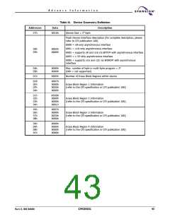
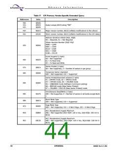
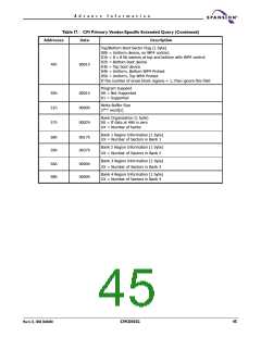
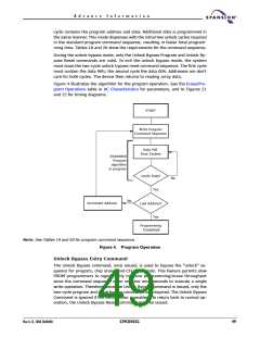
Tables 19–20 show all the commands executed by the device. The device auto-
matically powers up in the read/reset state. It is not necessary to issue a read/
reset command after power-up or hardware reset.
Read/Reset Command
After power-up or hardware reset, the device automatically enter the read state.
It is not necessary to issue the reset command after power-up or hardware reset.
Standard microprocessor cycles retrieve array data, however, after power-up,
only asynchronous accesses are permitted since the Configuration Register is at
its reset state with burst accesses disabled.
The Reset command is executed when the user needs to exit any of the other user
command sequences (such as autoselect, program, chip erase, etc.) to return to
reading array data. There is no latency between executing the Reset command
and reading array data.
The Reset command does not disable the SecSi sector if it is enabled. This func-
tion is only accomplished by issuing the SecSi Sector Exit command.
Autoselect Command
Flash memories are intended for use in applications where the local CPU alters
memory contents. As such, manufacturer and device codes must be accessible
while the device resides in the target system. PROM programmers typically ac-
cess the signature codes by raising A9 to V . However, multiplexing high voltage
ID
onto the address lines is not generally desired system design practice.
The device contains an Autoselect Command operation to supplement traditional
PROM programming methodology. The operation is initiated by writing the Au-
toselect command sequence into the command register. The bank address (BA)
is latched during the autoselect command sequence write operation to distinguish
which bank the Autoselect command references. Reading the other bank after the
Autoselect command is written results in reading array data from the other bank
and the specified address. Following the command write, a read cycle from ad-
dress (BA)XX00h retrieves the manufacturer code of (BA)XX01h. Three
sequential read cycles at addresses (BA) XX01h, (BA) XX0Eh, and (BA) XX0Fh
read the three-byte device ID (see Table 19).
(The Autoselect Command requires the user to execute the Read/Reset command
to return the device back to reading the array contents.)
Program Command Sequence
Programming is a four-bus-cycle operation. The program command sequence is
initiated by writing two unlock write cycles, followed by the program set-up com-
March 22, 2004 30606B0
S29CD032G
47

 SPANSION [ SPANSION ]