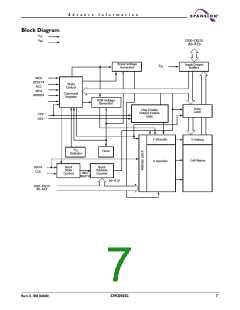
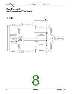
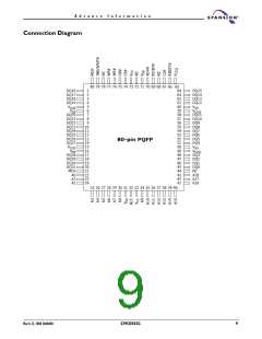
A d v a n c e I n f o r m a t i o n
Pin Configuration
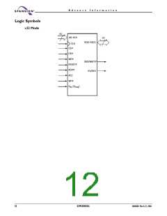
A0–A19
=
20-bit address bus for 32 Mb device. A9 supports 12
V autoselect inputs.
DQ0–DQ31
CE#
=
=
32-bit data inputs/outputs/float
Chip Enable Input. This signal is asynchronous
relative to CLK for the burst mode.
Output Enable Input. This signal is asynchronous
relative to CLK for the burst mode.
Write enable. This signal is asynchronous relative to
CLK for the burst mode.
OE#
WE#
=
=
V
NC
RY/BY#
=
=
=
Device ground
Pin not connected internally
Ready/Busy output and open drain. When RY/BY# =
SS
V , the device is ready to accept read operations
IH
and commands. When RY/BY# = V , the device is
OL
either executing an embedded algorithm or the
device is executing a hardware reset operation.
Clock Input that can be tied to the system or
microprocessor clock and provides the fundamental
timing and internal operating frequency.
CLK
=
ADV#
IND#
=
=
Load Burst Address input. Indicates that the valid
address is present on the address inputs.
End of burst indicator for finite bursts only. IND is low
when the last word in the burst sequence is at the
data outputs.
WAIT#
WP#
=
=
Provides data valid feedback only when the burst
length is set to continuous.
Write Protect input. When WP# = V , the two
OL
outermost bootblock sector in the 75% bank are
write protected regardless of other sector protection
configurations.
ACC
=
Acceleration input. When taken to 12 V, program and
erase operations are accelerated. When not used for
acceleration, ACC = V to V
.
SS
CC
V
V
(V
)
=
=
=
=
Output Buffer Power Supply (1.65 V to 2.75 V)
Chip Power Supply (2.5 V to 2.75 V)
Hardware reset input
IO
CCQ
CC
RESET#
MCH
Must Connect High (to V
)
CC
March 22, 2004 30606B0
S29CD032G
11

 SPANSION [ SPANSION ]