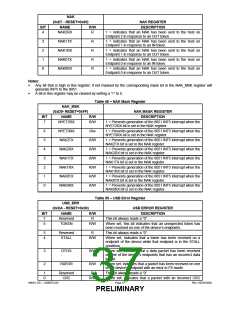
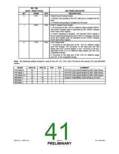
IDE_TIM
(0xDF - RESET=0x00)
IDE TIMING REGISTER
DESCRIPTION
BIT
NAME
R/W
2
PPE
R/W Prefetch and Posting Enable.
1:Prefetch and posting to the IDE data port is enabled for the
drive.
0: Prefetch and posting is disabled for the drive .
R/W IORDY Sample Point Enable.
1
ISPE
1: All accesses to the ATA I/O address range sample IORDY.
The IORDY sample point is specified by the “IORDY Sample
Point” field of this register.
0: IORDY sampling is disabled. The internal IORDY signal is
forced asserted guaranteeing that IORDY is sampled asserted
at the first sample point as specified by the “IORDY Sample
Point” field in this register.
0
FTB
R/W Fast Timing Bank.
1: Accesses to the data port of the ATA IO address range
uses fast timings. PIO accesses to the data port use fast
timing only if bit 3 of this register is zero. Accesses to all non-
data ports of the ATA I/O address range always use the 8 bit
compatible timings.
0: Accesses to the data port of the ATA I/O address range
uses the 16 bit compatible timing.
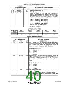
Note: the following settings should be used for the ISP, RT, DTE, and FTB bits for the various PIO and MWDMA
modes:
MODE
PIO Mode 0
PIO Mode 1
PIO Mode 2-4
MWDMA 0
MWDMA 1
MWDMA 2
ISP[1:0]
00
RT[1:0]
11
FTB
1
DTE
COMMENT
0
0
0
x
x
x
ATA PIO cycle speed limited by 8051 data moves
ATA PIO cycle speed limited by 8051 data moves
ATA PIO cycle speed limited by 8051 data moves
requires compatibility mode timing to be used
01
11
1
10
11
1
00
00
0
10
10
1
10
11
1
SMSC DS – USB97C201
Page 41
Rev. 03/25/2002
PRELIMINARY

 SMSC [ SMSC CORPORATION ]