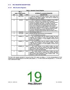
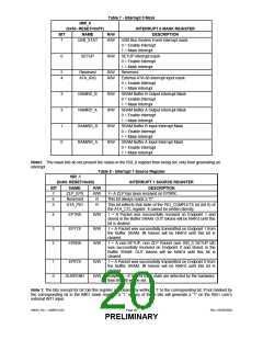
Table 7 - Interrupt 0 Mask
INTERRUPT 0 MASK REGISTER
IMR_0
(0x93- RESET=0xFF)
NAME
BIT
R/W
DESCRIPTION
USB Bus System Event interrupt mask
0 = Enable Interrupt
7
USB_STAT
R/W
1 = Mask Interrupt
6
SETUP
R/W
SETUP interrupt mask
0 = Enable Interrupt
1 = Mask Interrupt
5
4
Reserved
ATA_IRQ
R/W
R/W
Reserved.
External ATA-66 interrupt input mask
0 = Enable Interrupt
1 = Mask Interrupt
3
2
1
0
RAMRD_B
RAMRD_A
RAMWR_B
RAMWR_A
R/W
R/W
R/W
R/W
SRAM Buffer B Output Interrupt Mask
0 = Enable Interrupt
1 = Mask Interrupt
SRAM Buffer A Output Interrupt Mask
0 = Enable Interrupt
1 = Mask Interrupt
SRAM Buffer B Input Interrupt Mask
0 = Enable Interrupt
1 = Mask Interrupt
SRAM Buffer A Input Interrupt Mask
0 = Enable Interrupt
1 = Mask Interrupt
Note1: The mask bits do not prevent the status in the ISR_0 register from being set, only from generating an
interrupt.
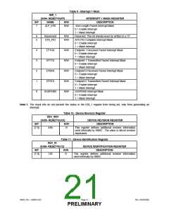
Table 8 - Interrupt 1 Source Register
ISR_1
(0x90- RESET=0x00)
INTERRUPT 1 SOURCE REGISTER
DESCRIPTION
BIT
7
NAME
R/W
ZLP_EP0
Reserved
ATA_PIO
R/W
R
1= A ZLP has been received on EP0RX.
6
This bit always reads a “0”.
5
R
This bit reflects that state of the PIO_COMPLETE bit (bit 6) of
the ATA_CTL register. It cannot be written directly.
4
3
2
EP1RX
EP1TX
EP0RX
R/W
R/W
R/W
1 = A Packet was successfully received on Endpoint 1 and
stored in the Buffer SRAM. OUT tokens will be NAK’d until this
bit is cleared.
1 = A Packet was successfully transmitted on Endpoint 1 from
the Buffer SRAM. IN tokens will be NAK’d until this bit is
cleared.
1 = A non-SETUP, non ZLP Packet (see ISR_0 SETUP bit)
was successfully received on Endpoint 0 and stored in the
Buffer SRAM. OUT tokens will be NAK’d until this bit is
cleared.
1
0
EP0TX
R/W
R/W
1 = A Packet was successfully transmitted on Endpoint 0 from
the Buffer SRAM. IN tokens will be NAK’d until this bit is
cleared.
SUSPEND
Suspend – If 3ms of IDLE state are detected by the hardware,
then this bit will be set.
Note 1: The bits (except for bit 5)in this register are cleared by writing a ‘1’ to the corresponding bit. If not masked by
the corresponding bit in the IMR1 mask register, a “1” on any of these bits will generate a “1” on the 8051 core’s
external INT1 input.
SMSC DS – USB97C201
Page 20
Rev. 03/25/2002
PRELIMINARY

 SMSC [ SMSC CORPORATION ]