6.1.4
MCU REGISTER DESCRIPTIONS
6.1.4.1 MCU Runtime Registers
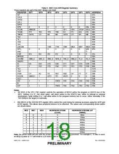
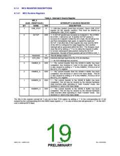
Table 6 - Interrupt 0 Source Register
ISR_0
(0x80 - RESET=0x0C)
INTERRUPT 0 SOURCE REGISTER
BIT
NAME
R/W
DESCRIPTION
7
USB_STAT
R
1= USB Bus System Event has occurred. Check USB_STAT
register for the specific event(s). This must be cleared by
clearing the USB_STAT register.
6
SETUP
R/W 1= A SETUP packet was received on Endpoint 0. The EP0RX
bit of ISR_1 will not be set. If another SETUP packet is
received on Endpoint 0 while this bit is high, the bit will go low
and then immediately high again, to signal the duplicate
SETUP. If all other bits in this register are clear and the INT0
of the 8051is configured for edge triggering, then another
interrupt will be generated within the 8051. The firmware must
clear this bit by writing a "1" to it to allow the Enpoint 0 buffer
to receive subsequent data packets during the SETUP
transaction. Receipt of these packets will set EP0RX in ISR_1.
5
4
Reserved
ATA_IRQ
R
This bit always reads a “0”.
R/W External interrupt input from the ATA-66 Interface.
1 = An ATA interrupt has occurred.
3
2
1
0
RAMRD_B
RAMRD_A
RAMWR_B
RAMWR_A
R/W 1 = The current transfer from the SRAM B Buffer has been
completed. See Sections 6.7 and 6.9 for more detail. This bit
is also cleared by writing a “1” to the RAMRD_TOGGLE bit of
the EP2_CTL register.
R/W 1 = The current transfer from the SRAM A Buffer has been
completed. See Sections 6.7 and 6.9 for more detail. . This bit
is also cleared by writing a “0” to the RAMRD_TOGGLE bit of
the EP2_CTL register.
R/W 1 = The current transfer to the SRAM B Buffer has been
completed. This bit may be cleared by the internal hardware
state machine while operating in “Auto Transfer” mode. See
Sections 6.7 and 6.9 for more detail.
R/W 1 = The current transfer to the SRAM A Buffer has been
completed. This bit may be cleared by the internal hardware
state machine while operating in “Auto Transfer” mode. See
Sections 6.7 and 6.9 for more detail.
The bits in this register (except bit 7) are set to their POR values by writing a ‘1’ to the corresponding bit. If not
masked by the corresponding bit in the IMR0 mask register, a “1” on any of these bits will generate a “1” on the 8051
core’s external INT0 input.
SMSC DS – USB97C201
Page 19
Rev. 03/25/2002
PRELIMINARY

 SMSC [ SMSC CORPORATION ]