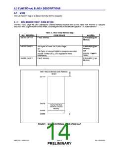
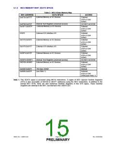
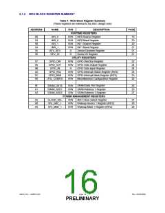
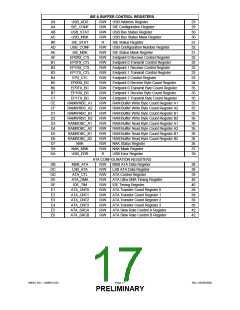
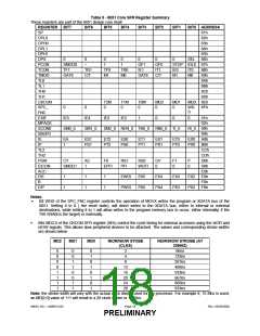
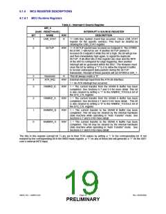
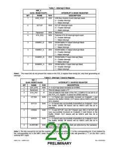
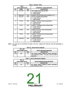
Table 5 - 8051 Core SFR Register Summary
These registers are part of the 8051 design core itself.
REGISTER BIT7
BIT6
BIT5
BIT4
BIT3
BIT2
BIT1
BIT0 ADDRESS
SP
81h
82h
83h
84h
85h
DPL0
DPH0
DPL1
DPH1
DPS
PCON
TCON
TMOD
TL0
0
0
0
0
0
0
0
SEL
86h
SMOD0
TF1
–
1
1
GF1
IE1
GF0
IT1
C/T
STOP IDLE 87h
TR1
C/T
TF0
M1
TR0
M0
IE0
M1
IT0
M0
88h
89h
8Ah
8Bh
8Ch
8Dh
GATE
GATE
TL1
TH0
TH1
CKCON
SPC_
FNC
EXIF
MPAGE
SCON0
SBUF0
IE
T2M
0
T1M
0
T0M
0
MD2
0
MD1
0
MD0 8Eh
0
0
WR
S
8Fh
IE5
IE4
IE3
IE2
1
0
0
0
91h
92h
SM0_0
SM1_0
SM2_0 REN_0 TB8_0
RB8_0 TI_0
RI_0 98h
99h
EA
1
ES1
PS1
ET2
PT2
ES0
PS0
ET1
PT1
EX1
PX1
ET0
PT0
EX0
PX0
A8h
B8h
CCh
CDh
D0h
D8h
E0h
E8h
F0h
F8h
IP
TL2
TH2
PSW
EICON
ACC
EIE
CY
AC
1
F0
RS1
PFI
RS0
OV
0
F1
0
P
0
SMOD1
EPFI
WDTI
1
1
1
1
1
1
EWDI
PWDI
EX5
PX5
EX4
PX4
EX3
PX3
EX2
PX2
B
EIP
Notes:
ꢀ
Bit WRS of the SPC_FNC register controls the operation of MOVX writes the program or XDATA bus of the
8051. Setting it to 0 ( the reset state), will direct writes to the XDATA bus, either to internal or external
destinations, while setting it to 1 will allow writes to the program memory bus to occur, either internally( if the
768 SRAM is the target) or externally.
ꢀ
Bits MD2:0 of the CKCON SFR register (8Eh) control the cycle timing for external accesses using the nIOR and
nIOW signals. This allows slow peripheral devices to be attached. The values and corresponding strobe widths
are shown below:
MD2
MD1
MD0
NIOR/NIOW STOBE
(CLKS)
NIOR/NIOW STROBE (AT
30MHZ)
0
0
0
0
1
1
1
1
0
0
1
1
0
0
1
1
0
1
0
1
0
1
0
1
2
66ns
133ns
267ns
400ns
533ns
667ns
800ns
933ns
4
8
12
16
20
24
28
Note: the strobe width will vary with the actual clock divider used for the processor. For example if, 16 Mhz is used,
an MD[2:0] value of 111 will result in a 28 clock strobe or 1866ns.
SMSC DS – USB97C201
Page 18
Rev. 03/25/2002
PRELIMINARY

 SMSC [ SMSC CORPORATION ]