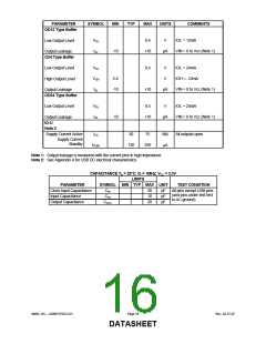
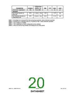
PARAMETER
SYMBOL
MIN
TYP
MAX
UNITS
COMMENTS
OD12 Type Buffer
VOL
IOL
0.4
V
IOL = 12mA
Low Output Level
-10
+10
µA
VIN = 0 to Vcc (Note 1)
Output Leakage
O24 Type Buffer
VOL
VOH
IOL
0.4
V
V
IOL = 24mA
Low Output Level
High Output Level
2.4
-10
IOH = -12mA
+10
µA
VIN = 0 to Vcc (Note 1)
Output Leakage
OD24 Type Buffer
VOL
IOL
0.4
V
IOL = 24mA
Low Output Level
-10
+10
µA
VIN = 0 to Vcc (Note 1)
Output Leakage
IO-U
Note 2
Supply Current Active
ICC
30
75
MA
All outputs open.
Supply Current
Standby
ICSBU
120
250
μA
Note 1: Output leakage is measured with the current pins in high impedance.
Note 2: See Appendix A for USB DC electrical characteristics.
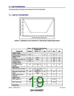
CAPACITANCE TA = 25°C; fc = 1MHz; VCC = 3.3V
LIMITS
PARAMETER
Clock Input Capacitance
Input Capacitance
SYMBOL MIN TYP MAX UNIT
TEST CONDITION
CIN
CIN
20
10
20
pF
pF
pF
All pins except USB pins
(and pins under test tied
to AC ground)
Output Capacitance
COUT
SMSC DS – USB97CFDC2-01
Page 16
Rev. 02-27-07
DATASHEET

 SMSC [ SMSC CORPORATION ]