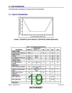
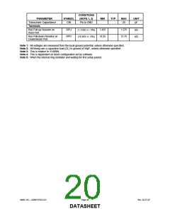
CONDITIONS
(NOTE 1, 2)
Pin to GND
PARAMETER
Transceiver Capacitance
Terminals
SYMBOL
MIN
TYP
MAX
UNIT
CIN
20
pF
Bus Pull-up Resistor on
Root Port
RPU
RPD
1.425
14.25
1.575
15.75
(1.5 KΩ +/- 5%)
(15 KΩ +/- 5%)
kΩ
kΩ
Bus Pull-down Resistor on
Downstream Port
Note 1: All voltages are measured from the local ground potential, unless otherwise specified.
Note 2: All timing use a capacitive load (CL) to ground of 50pF, unless otherwise specified.
Note 3: This is relative to VUSBIN.
Note 4: This is dependent on block configuration set by software.
Note 5: When the internal ring oscillator and waiting for first setup packet.
SMSC DS – USB97CFDC2-01
Page 20
Rev. 02-27-07
DATASHEET

 SMSC [ SMSC CORPORATION ]