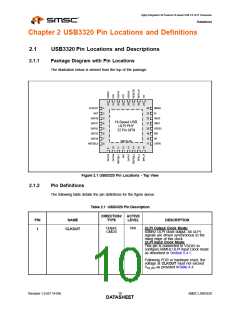
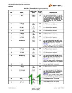
Highly Integrated Full Featured Hi-Speed USB 2.0 ULPI Transceiver
Datasheet
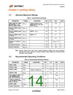
Chapter 3 Limiting Values
3.1
Absolute Maximum Ratings
Table 3.1 Absolute Maximum Ratings
PARAMETER
SYMBOL
CONDITIONS
MIN
TYP
MAX
UNITS
VBUS, VBAT, ID, CPEN, VMAX_5V
DP, DM, SPK_L, and
SPK_R voltage to GND
Voltage measured at pin.
-0.5
+6.0
V
VBUS tolerant to 30V with
external RVBUS.
Maximum VDD18 voltage VMAX_18V
-0.5
-0.5
-0.5
-0.5
-0.5
2.5
4.0
V
V
V
V
V
to Ground
Maximum VDDIO voltage VMAX_IOV
to Ground
VDD18 = VDD18
VDD18 = 0V
Maximum VDDIO voltage VMAX_IOV
to Ground
0.7
Maximum VDD33 voltage VMAX_33V
to Ground
4.0
Maximum I/O voltage to
Ground
VMAX_IN
VDDIO + 0.7
Operating Temperature
Storage Temperature
TMAX_OP
-40
-55
85
°C
°C
TMAX_STG
150
Note: Stresses beyond those listed under “Absolute Maximum Ratings” may cause permanent
damage to the device. Exposure to absolute maximum rating conditions for extended periods
may affect device reliability.
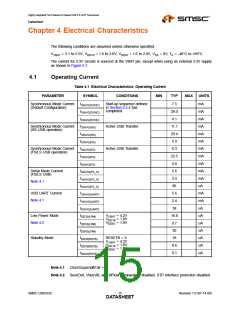
3.2
Recommended Operating Conditions
Table 3.2 Recommended Operating Conditions
PARAMETER
SYMBOL
CONDITIONS
MIN
TYP
MAX
UNITS
VBAT to GND
VDD33 to GND
VDDIO to GND
VVBAT
VDD33
VDDIO
3.1
3.0
1.6
5.5
3.6
3.6
V
V
V
3.3
1.8-3.3
VDDIO ≥ VDD18(min)
VDD18 to GND
VDD18
VI
1.6
0.0
1.8
2.0
V
V
Input Voltage on Digital
Pins (RESETB, STP,
DIR, NXT, DATA[7:0])
VDDIO
Voltage on Analog I/O
Pins (DP, DM, ID, CPEN,
SPK_L, SPK_R)
VI(I/O)
0.0
VDD33
V
VBUS to GND
VVMAX
TA
0.0
-40
5.5
85
V
Ambient Temperature
°C
Revision 1.0 (07-14-09)
SMSC USB3320
DATA1S4HEET

 SMSC [ SMSC CORPORATION ]