Highly Integrated Full Featured Hi-Speed USB 2.0 ULPI Transceiver
Datasheet
Chapter 2 USB3320 Pin Locations and Definitions
2.1
USB3320 Pin Locations and Descriptions
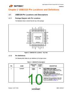
2.1.1
Package Diagram with Pin Locations
The illustration below is viewed from the top of the package.
CLKOUT
NXT
1
2
3
4
5
6
7
8
24
23
22
21
20
19
18
17
RBIAS
ID
DATA0
DATA1
DATA2
DATA3
DATA4
REFSEL0
VBUS
VBAT
VDD33
DM
USB3300
Hi-Speed USB
Hi-Speed USB2
ULPI PHY
ULPI PHY
32 Pin QFN
32 Pin QFN
DP
GND FLAG
CPEN
Figure 2.1 USB3320 Pin Locations - Top View
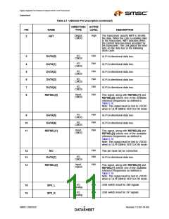
2.1.2
Pin Definitions
The following table details the pin definitions for the figure above.
Table 2.1 USB3320 Pin Description
DIRECTION/ ACTIVE
PIN
1
NAME
TYPE
LEVEL
DESCRIPTION
Output,
CMOS
N/A
ULPI Output Clock Mode:
CLKOUT
60MHz ULPI clock output. All ULPI
signals are driven synchronous to the
rising edge of this clock.
ULPI Input Clock Mode:
This pin is connected to VDDIO to
configure 60MHz ULPI Input Clock mode
as described in Section 5.4.1.
Following POR or hardware reset, the
voltage at CLKOUT must not exceed
VIH_ED as provided inTable 4.4.
Revision 1.0 (07-14-09)
SMSC USB3320
DATA1S0HEET

 SMSC [ SMSC CORPORATION ]