Highly Integrated Full Featured Hi-Speed USB 2.0 ULPI Transceiver
Datasheet
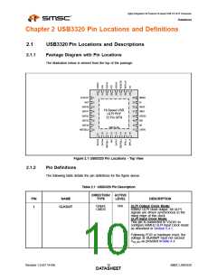
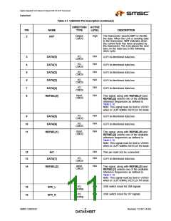
Table 2.1 USB3320 Pin Description (continued)
DIRECTION/ ACTIVE
PIN
2
NAME
NXT
TYPE
LEVEL
DESCRIPTION
Output,
CMOS
High
The transceiver asserts NXT to throttle
the data. When the Link is sending data
to the transceiver, NXT indicates when
the current byte has been accepted by
the transceiver. The Link places the next
byte on the data bus in the following
clock cycle.
I/O,
N/A
N/A
N/A
N/A
N/A
N/A
3
4
5
6
7
8
DATA[0]
DATA[1]
DATA[2]
DATA[3]
DATA[4]
REFSEL[0]
ULPI bi-directional data bus.
ULPI bi-directional data bus.
ULPI bi-directional data bus.
ULPI bi-directional data bus.
ULPI bi-directional data bus.
CMOS
I/O,
CMOS
I/O,
CMOS
I/O,
CMOS
I/O,
CMOS
Input,
CMOS
This signal, along with REFSEL[1] and
REFSEL[2] selects one of the available
reference frequencies as defined in
Table 5.10.
Note: This signal must be tied to VDDIO
when in ULPI 60MHz REFCLK IN mode.
I/O,
N/A
N/A
N/A
9
DATA[5]
DATA[6]
ULPI bi-directional data bus.
ULPI bi-directional data bus.
CMOS
I/O,
CMOS
10
11
Input,
CMOS
REFSEL[1]
This signal, along with REFSEL[0] and
REFSEL[2] selects one of the available
reference frequencies as defined in
Table 5.10.
Note: This signal must be tied to VDDIO
when in ULPI 60MHz REFCLK IN mode.
N/A
N/A
12
13
N/C
This pin must not be connected.
ULPI bi-directional data bus.
I/O,
CMOS
DATA[7]
Input,
CMOS
N/A
14
REFSEL[2]
This signal, along with REFSEL[0] and
REFSEL[1] selects one of the available
reference frequencies as defined in
Table 5.10.
Note: This signal must be tied to VDDIO
when in ULPI 60MHz REFCLK IN mode.
I/O,
N/A
N/A
USB switch in/out for DM signals
USB switch in/out for DP signals
15
16
SPK_L
SPK_R
Analog
I/O,
Analog
SMSC USB3320
Revision 1.0 (07-14-09)
DATAS11HEET

 SMSC [ SMSC CORPORATION ]