Highly Integrated Full Featured Hi-Speed USB 2.0 ULPI Transceiver
Datasheet
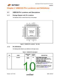
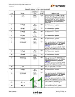
Table 2.1 USB3320 Pin Description (continued)
DIRECTION/ ACTIVE
PIN
29
NAME
STP
TYPE
LEVEL
DESCRIPTION
Input,
CMOS
High
The Link asserts STP for one clock cycle
to stop the data stream currently on the
bus. If the Link is sending data to the
transceiver, STP indicates the last byte of
data was on the bus in the previous
cycle.
Power
N/A
N/A
External 1.8V Supply input pin. This pad
needs to be bypassed with a 0.1uF
capacitor to ground, placed as close as
possible to the USB3320.
30
31
VDD18
DIR
Output,
CMOS
Controls the direction of the data bus.
When the transceiver has data to transfer
to the Link, it drives DIR high to take
ownership of the bus. When the
transceiver has no data to transfer it
drives DIR low and monitors the bus for
commands from the Link.
Power
N/A
N/A
External 1.8V to 3.3V ULPI supply input
pin. This voltage sets the value of VOH for
the ULPI signals. This pad needs to be
bypassed with a 0.1uF capacitor to
ground, placed as close as possible to
the USB3320.
32
VDDIO
GND
Ground
Ground.
FLAG
SMSC USB3320
Revision 1.0 (07-14-09)
DATA1S3HEET

 SMSC [ SMSC CORPORATION ]