4th Generation USB2.0 Flash Media Controller with Integrated Card Power FETs and HS Hub
Datasheet
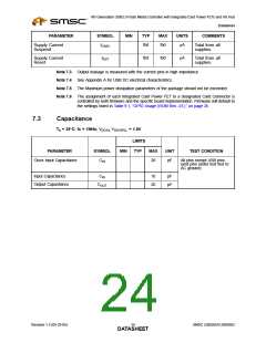
PARAMETER
SYMBOL
MIN
TYP
MAX
UNITS
COMMENTS
ICSBY
tbd
tbd
µA
Supply Current
Total from all
supplies.
Suspend
IRST
tbd
tbd
µA
Supply Current
Reset
Total from all
supplies.
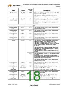
Note 7.3 Output leakage is measured with the current pins in high impedance.
Note 7.4 See Appendix A for USB DC electrical characteristics.
Note 7.5 The Maximum power dissipation parameters of the package should not be exceeded
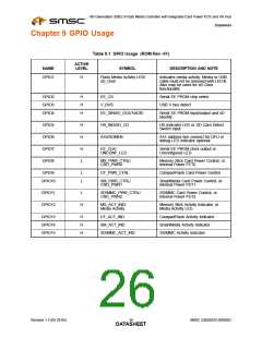
Note 7.6 The assignment of each Integrated Card Power FET to a designated Card Connector is
controlled by both firmware and the specific board implementation. Firmware will default to
the settings listed in Table 9.1, “GPIO Usage (ROM Rev -01),” on page 26
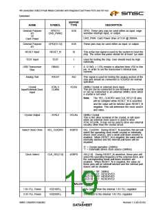
7.3
Capacitance
TA = 25°C; fc = 1MHz; VDD18, VDD18PLL = 1.8V
LIMITS
PARAMETER
SYMBOL
MIN
TYP
MAX
UNIT
TEST CONDITION
Clock Input Capacitance
CIN
20
pF
All pins except USB pins
(and pins under test tied to
AC ground)
Input Capacitance
Output Capacitance
CIN
10
20
pF
pF
COUT
Revision 1.3 (05-25-05)
SMSC USB2601/USB2602
DATA2S4HEET

 SMSC [ SMSC CORPORATION ]