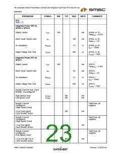
4th Generation USB2.0 Flash Media Controller with Integrated Card Power FETs and HS Hub
Datasheet
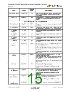
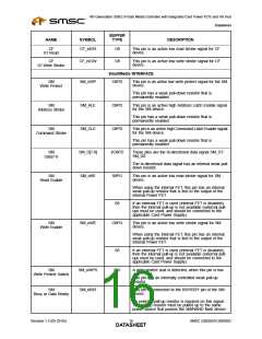
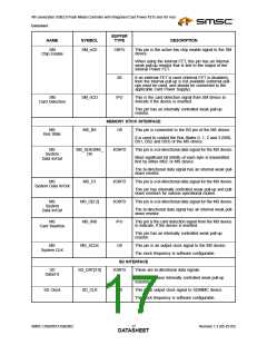
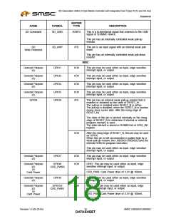
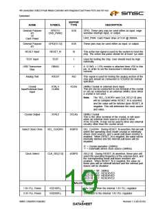
BUFFER
NAME
SYMBOL
TYPE
DESCRIPTION
General Purpose
GPIO11/
I/O8
GPIO: These pins may be used either as input, edge
sensitive interrupt input, or output.
I/O
Or
CRD_PWR2
CRD_PWR: Card Power drive of 3.3V @ 200mA.
These pins may be used either as input, or output.
Card Power
General Purpose
I/O
GPIO[15:12]
RESET_N
TEST
I/O8
RESET input
IS
I
This active low signal is used by the system to reset the
chip. The active low pulse should be at least 1µs wide.
TEST Input
Used for testing the chip. User should must tie high
externally.
USB Transceiver
Bias
RBIAS
I
A 12.0kΩ, ± 1.0% resistor is attached from VSS to this
pin, in order to set the transceiver’s internal bias
currents.
Analog Test
ATEST
AIO
This signal is used for testing the analog section of the
chip and should be connected to VDDA33 for normal
operation.
Crystal
Input/External Clock
Input
XTAL1/
CLKIN
ICLKx
24Mhz Crystal or external clock input.
This pin can be connected to one terminal of the crystal
or can be connected to an external 24Mhz clock when
a crystal is not used.
Note:
The ‘SEL_CLKDRV and CLK_SEL[1:0]’ pins
will be sampled while RESET_N is asserted,
and the value will be latched upon RESET_N
negation. This will determine the clock source
and value.
Crystal Output
XTAL2
OCLKx
I/O8PD
24Mhz Crystal
This is the other terminal of the crystal, or left open
when an external clock source is used to drive
XTAL1/CLKIN. It may not be used to drive any external
circuitry other than the crystal circuit.
Select Clock Drive
SEL_CLKDRV
SEL_CLKDRV. During RESET_N assertion, this pin will
select the operating clock mode (crystal or externally
driven clock source), and a weak pull-down resistor is
enabled. When RESET_N is negated, the value will be
internally latched and the internal pull-down will be
disabled.
‘0’ = Crystal operation (24MHz)
‘1’ = Externally driven clock source (24MHz)
Clock Select
CLK_SEL[1:0]
I/O8PD
SEL[1:0]. During RESET_N assertion, these pins will
select the operating frequency of the external clock, and
the corresponding weak pull-down resistors are
enabled. When RESET_N is negated, the value on
these pins will be internal latched and the internal pull-
downs will be disabled.
SEL[1:0] = ‘00’. 24MHz
SEL[1:0] = ‘01’. RESERVED
SEL[1:0] = ‘10’. RESERVED
SEL[1:0] = ‘11’. RESERVED
ANALOG POWER
1.8V PLL Power
3.3V PLL Power
VDD18PLL
VDD33PLL
1.8v Output from the internal 1.8V PLL regulator
3.3V Input to the internal 1.8V PLL regulator.
SMSC USB2601/USB2602
Revision 1.3 (05-25-05)
DATA1S9HEET

 SMSC [ SMSC CORPORATION ]