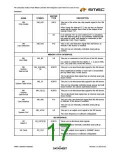
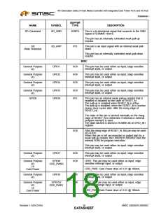
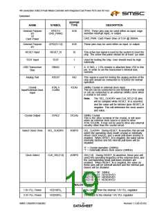
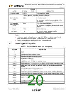
4th Generation USB2.0 Flash Media Controller with Integrated Card Power FETs and HS Hub
Datasheet
Chapter 7 DC Parameters
7.1
Maximum Guaranteed Ratings
Operating Temperature Range ............................................................................................0oC to +70oC
Storage Temperature Range.............................................................................................-55o to +150oC
Lead Temperature Range (soldering, 10 seconds)...................................................................... +325oC
Positive Voltage on GPIO3, with respect to Ground......................................................................... 5.5V
Positive Voltage on any signal pin, with respect to Ground ............................................................. 4.6V
Positive Voltage on XTAL1, with respect to Ground......................................................................... 4.0V
Positive Voltage on XTAL2, with respect to Ground......................................................................... 2.5V
Negative Voltage on GPIO8, 10 & 11, with respect to Ground (see Note 7.2)...............................-0.5V
Negative Voltage on any pin, with respect to Ground .....................................................................-0.5V
Maximum VDD18, VDD18PLL .............................................................................................................. +2.5V
Maximum VDD33, VDDA33 ................................................................................................................. +4.6V
*Stresses above the specified parameters could cause permanent damage to the device. This is a
stress rating only and functional operation of the device at any other condition above those indicated
in the operation sections of this specification is not implied.
Note 7.1 When powering this device from laboratory or system power supplies, it is important that
the Absolute Maximum Ratings not be exceeded or device failure can result. Some power
supplies exhibit voltage spikes on their outputs when the AC power is switched on or off.
In addition, voltage transients on the AC power line may appear on the DC output. When
this possibility exists, it is suggested that a clamp circuit be used.
Note 7.2 When internal power FET operation of these pins is enabled, these pins may be
simultaneously shorted to ground or any voltage up to 3.63V indefinitely, without damage
to the device as long as VDD33 and VDDA33 are less than 3.63V and TA is less than 70°C.
7.2
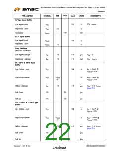
DC Electrical Characteristics
(TA = 0°C - 70°C, VDD33, VDDA33 = +3.3 V ± 0.3 V, VDD18, VDD18PLL = +1.8 V ± 10%,)
PARAMETER
SYMBOL
MIN
TYP
MAX
UNITS
COMMENTS
I,IPU & IPD Type Input Buffer
Low Input Level
High Input Level
Pull Down
VILI
VIHI
PD
PU
0.8
V
V
TTL Levels
2.0
72
58
µA
µA
Pull Up
SMSC USB2601/USB2602
Revision 1.3 (05-25-05)
DATA2S1HEET

 SMSC [ SMSC CORPORATION ]