4th Generation USB2.0 Flash Media Controller with Integrated Card Power FETs and HS Hub
Datasheet
BUFFER
NAME
SYMBOL
TYPE
DESCRIPTION
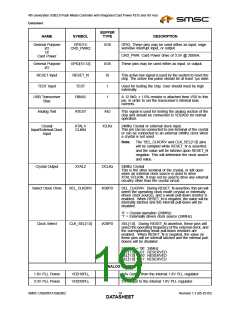
3.3v Analog PHY Power
3.3V Analog Power
VDDA33
DIGITAL POWER, GROUNDS, and NO CONNECTS
1.8v Digital Core
Power
VDD18
+1.8V Core power
All VDD18 pins must be connected together on the
circuit board.
3.3v Power & &
Voltage Regulator
Input
VDD33
3.3V Power & Regulator Input.
pin 87 supplies 3.3V power to the internal 1.8V VDD18
regulator.
Ground
VSS
NC
Ground Reference
No Connect
No Connect. No trace or signal should be
routed/attached to these pins.
Notes:
■
Hot-insertion capable card connectors are required for all flash media. It is required for SD
connector to have Write Protect switch. This allows the chip to detect MMC card.
■
nMCE is normally asserted except when the 8051 is in standby mode.
6.2
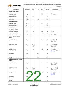
Buffer Type Descriptions
Table 6.1 USB2601/USB2602 Buffer Type Descriptions
BUFFER
DESCRIPTION
I
Input
IPU
Input with internal weak pull-up resistor.
IPD
Input with internal weak pull-down resistor.
IS
Input with Schmitt trigger
I/O8
I/O8PU
I/O8PD
Input/Output buffer with 8mA sink and 8mA source.
Input/Output buffer with 8mA sink and 8mA source, with an internal weak pull-up resistor.
Input/Output buffer with 8mA sink and 8mA source, with an internal weak pull-down
resistor.
O8
Output buffer with 8mA sink and 8mA source.
Output buffer with 8mA sink and 8mA source, with an internal weak pull-up resistor.
Output buffer with 8mA sink and 8mA source, with an internal weak pull-down resistor.
XTAL clock input
O8PU
O8PD
ICLKx
OCLKx
I/O-U
AIO
XTAL clock output
Analog Input/Output Defined in USB specification
Analog Input/Output
Revision 1.3 (05-25-05)
SMSC USB2601/USB2602
DATA2S0HEET

 SMSC [ SMSC CORPORATION ]