5th Generation Hi-Speed USB Flash Media and CIR Controller with Integrated Card Power FETs
Datasheet
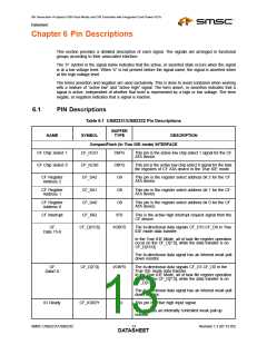
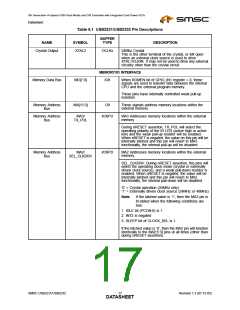
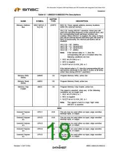
Table 6.1 USB2231/USB2232 Pin Descriptions
BUFFER
NAME
SYMBOL
TYPE
DESCRIPTION
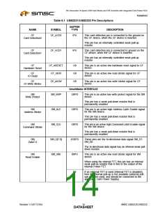
Crystal Output
XTAL2
OCLKx
24Mhz Crystal
This is the other terminal of the crystal, or left open
when an external clock source is used to drive
XTAL1/CLKIN. It may not be used to drive any external
circuitry other than the crystal circuit.
MEMORY/IO INTERFACE
Memory Data Bus
MD[7:0]
IO8
When ROMEN bit of GPIO_IN1 register = 0, these
signals are used to transfer data between the internal
CPU and the external program memory.
These pins have internally controlled weak pull-up
resistors.
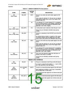
Memory Address
Bus
MA[15:3]
O8
These signals address memory locations within the
external memory.
Memory Address
Bus
MA3/
I/O8PU
MA3 Addresses memory locations within the external
memory.
TX_POL
During nRESET assertion, TX_POL will select the
operating polarity of the IR LED (active high or active
low) and the weak pull-up resistor will be enabled.
When nRESET is negated, the value on this pin will be
internally latched and this pin will revert to MA3
functionality, the internal pull-up will be disabled.
Memory Address
Bus
MA2/
I/O8PD
MA2 Addresses memory locations within the external
memory.
SEL_CLKDRV
SEL_CLKDRV. During nRESET assertion, this pins will
select the operating clock mode (crystal or externally
driven clock source), and a weak pull-down resistor is
enabled. When nRESET is negated, the value will be
internally latched and this pin will revert to MA2
functionality, the internal pull-down will be disabled.
‘0’ = Crystal operation (24MHz only)
‘1’ = Externally driven clock source (24MHz or 48MHz)
Note:
If the latched value is ‘1’, then the MA2 pin is
tri-stated when the following conditions are
true:
1. IDLE bit (PCON.0) is 1.
2. INT2 is negated
3. SLEEP bit of CLOCK_SEL is 1.
If the latched value is ‘0’, then the MA2 pin will function
identically to the MA[15:3] pins at all times (other than
during nRESET assertion).
SMSC USB2231/USB2232
Revision 1.3 (07-12-05)
DATA1S7HEET

 SMSC [ SMSC CORPORATION ]