5th Generation Hi-Speed USB Flash Media and CIR Controller with Integrated Card Power FETs
Datasheet
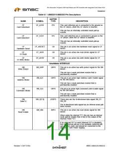
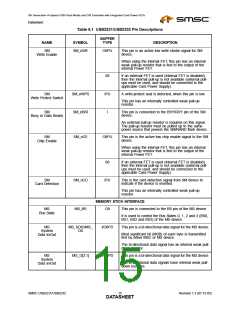
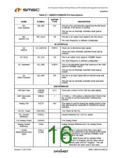
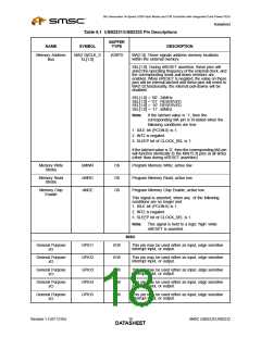
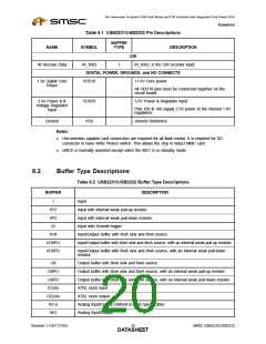
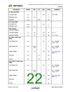
Table 6.1 USB2231/USB2232 Pin Descriptions
BUFFER
NAME
SYMBOL
TYPE
DESCRIPTION
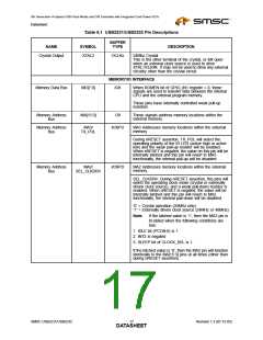
Memory Address
Bus
MA[1:0]/CLK_S
EL[1:0]
I/O8PD
MA[1:0], These signals address memory locations
within the external memory.
SEL[1:0]. During nRESET assertion, these pins will
select the operating frequency of the external clock, and
the corresponding weak pull-down resistors are
enabled. When nRESET is negated, the value on these
pins will be internal latched and these pins will revert to
MA[1:0] functionality, the internal pull-downs will be
disabled.
SEL[1:0] = ‘00’. 24MHz
SEL[1:0] = ‘01’. RESERVED
SEL[1:0] = ‘10’. RESERVED
SEL[1:0] = ‘11’. 48MHz
Note:
If the latched value is ‘1’, then the
corresponding MA pin is tri-stated when the
following conditions are true:
1. IDLE bit (PCON.0) is 1.
2. INT2 is negated
3. SLEEP bit of CLOCK_SEL is 1.
If the latched value is ‘0’, then the corresponding MA pin
will function identically to the MA[15:3] pins at all times
(other than during nRESET assertion).
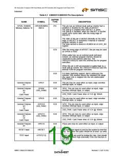
Memory Write
Strobe
nMWR
nMRD
nMCE
O8
O8
O8
Program Memory Write; active low
Program Memory Read; active low
Program Memory Chip Enable; active low.
Memory Read
Strobe
Memory Chip
Enable
This signal is asserted, when any of the following
conditions are no longer met:
1. IDLE bit (PCON.0) is 1.
2. INT2 is negated
3. SLEEP bit of CLOCK_SEL is 1.
Note:
This signal is held to a logic ‘high’ while
nRESET is asserted.
MISC
General Purpose
I/O
GPIO1
GPIO2
GPIO3
GPIO4
GPIO5
I/O8
I/O8
I/O8
I/O8
I/O8
This pin may be used either as input, edge sensitive
interrupt input, or output.
General Purpose
I/O
This pin may be used either as input, edge sensitive
interrupt input, or output.
General Purpose
I/O
This pin may be used either as input, edge sensitive
interrupt input, or output.
General Purpose
I/O
This pin may be used either as input, edge sensitive
interrupt input, or output.
General Purpose
I/O
This pin may be used either as input, edge sensitive
interrupt input, or output.
Revision 1.3 (07-12-05)
SMSC USB2231/USB2232
DATA1S8HEET

 SMSC [ SMSC CORPORATION ]