5th Generation Hi-Speed USB Flash Media and CIR Controller with Integrated Card Power FETs
Datasheet
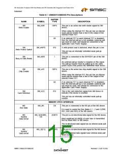
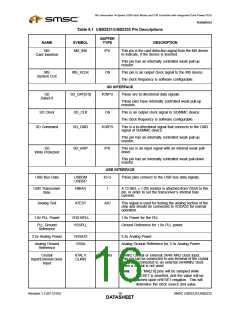
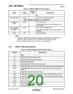
Table 6.1 USB2231/USB2232 Pin Descriptions
BUFFER
NAME
SYMBOL
TYPE
DESCRIPTION
MS
MS_INS
IPU
This pin is the card detection signal from the MS device
to indicate, if the device is inserted.
Card Insertion
This pin has an internally controlled weak pull-up
resistor.
MS
MS_SCLK
O8
This pin is an output clock signal to the MS device.
The clock frequency is software configurable.
System CLK
SD INTERFACE
SD
SD_DAT[3:0]
I/O8PU
These are bi-directional data signals.
Data3-0
These pins have internally controlled weak pull-up
resistors.
SD Clock
SD_CLK
SD_CMD
O8
This is an output clock signal to SD/MMC device.
The clock frequency is software configurable.
SD Command
I/O8PU
This is a bi-directional signal that connects to the CMD
signal of SD/MMC device.
This pin has an internally controlled weak pull-up
resistor.
SD
SD_nWP
IPD
This pin is an input signal with an internal weak pull-
down.
Write Protected
This pin has an internally controlled weak pull-down
resistor.
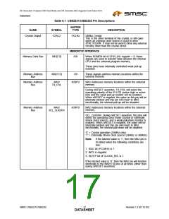
USB INTERFACE
USB Bus Data
USBDM
USBDP
IO-U
These pins connect to the USB bus data signals.
USB Transceiver
Bias
RBIAS
I
A 12.0kΩ, ± 1.0% resistor is attached from VSSA to this
pin, in order to set the transceiver’s internal bias
currents.
Analog Test
ATEST
AIO
This signal is used for testing the analog section of the
chip and should be connected to VDDA33 for normal
operation.
1.8v PLL Power
VDD18PLL
VSSPLL
1.8v Power for the PLL
PLL Ground
Reference
Ground Reference for 1.8v PLL power
3.3v Analog Power
VDDA33
VSSA
3.3v Analog Power
Analog Ground
Reference
Analog Ground Reference for 3.3v Analog Power.
Crystal
Input/External Clock
Input
XTAL1/
CLKIN
ICLKx
24Mhz Crystal or external 24/48 MHz clock input.
This pin can be connected to one terminal of the crystal
or can be connected to an external 24/48Mhz clock
when a crystal is not used.
Note:
The ‘MA[2:0] pins will be sampled while
nRESET is asserted, and the value will be
latched upon nRESET negation. This will
determine the clock source and value.
Revision 1.3 (07-12-05)
SMSC USB2231/USB2232
DATA1S6HEET

 SMSC [ SMSC CORPORATION ]