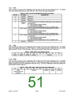
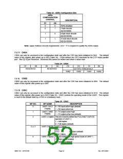
Table 33 - ADRx Configuration Bits
ADRx
CONFIGURATION
CONTROL
DESCRIPTION
D7
0
0
D6
0
1
ADRx disabled
1 Byte decode
A[3:0]=0000b
1
1
0
1
8 Byte block decode
A[3:0]=0XXXb
16 byte block decode
A[3:0]=XXXXb
Note: Upper Address Decode requirements: nCS = ’0’ is required to qualify the ADRx output.
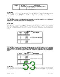
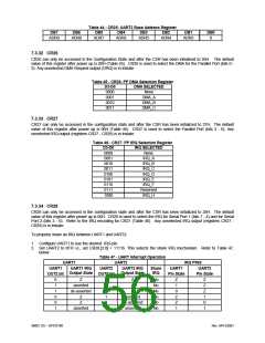
7.3.11 CR0A
CR0A can only be accessed in the configuration state and after the CSR has been initialized to 0AH. The default
value of this register after power up is 00H (Table 34). CR0A defines the FIFO threshold for the ECP mode parallel
port. Bits D[7:4] are Reserved. Reserved Bits cannot be written and return 0 when read.
Table 34 - CR0A
D7
D6
D5
D4
D3
D2
ECP FIFO THRESHOLD
THR2 THR1
D1
D0
RESERVED
RESERVED
THR3
THR0
7.3.12 CR0B
CR0B can only be accessed in the configuration state and after the CSR has been initialized to 0BH. The default
value of this register after power up is 00H.
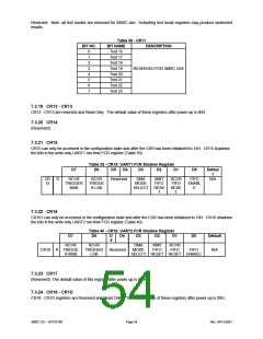
7.3.13 CR0C
CR0C can only be accessed in the configuration state and after the CSR has been initialized to 0CH. The default
value of this register after power up is 02H (Table 35). CR0C controls the operating mode of the UART. This register
is reset to the default state by a POR or a hardware reset.
Table 35 - CR0C
BIT NO.
BIT NAME
DESCRIPTION
0
UART 2 RCV 0 = RX input active high (default).
Polarity
1 = RX input active low.
1
2
UART 2 XMIT 0 = TX output active high.
Polarity
1 = TX output active low (default).
UART 2 Duplex This bit is used to define the FULL/HALF DUPLEX
operation of UART 2.
1 = Half duplex
0 = Full duplex (default)
UART 2 MODE UART 2 Mode
5 4 3
3, 4, 5
6
0 0 0
Standard (default)
Reserved
Other Values
UART 1 Speed This bit enables the high speed mode of UART 1.
1 = High speed enabled
0 = Standard (default)
SMSC DS – SP37E760
Page 52
Rev. 04/13/2001

 SMSC [ SMSC CORPORATION ]