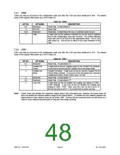
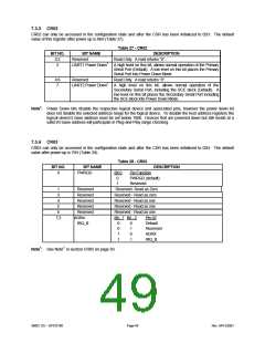
7.3.3 CR02
CR02 can only be accessed in the configuration state and after the CSR has been initialized to 02H. The default
value of this register after power up is 88H (Table 27).
Table 27 - CR02
BIT NO.
BIT NAME
Reserved
DESCRIPTION
0:2
3
Read Only. A read returns “0”.
UART1 Power Down1 A high level on this bit, allows normal operation of the Primary
Serial Port (Default). A low level on this bit places the Primary
Serial Port into Power Down Mode.
4:6
7
Reserved
Read Only. A read returns “0”.
UART2 Power Down1 A high level on this bit, allows normal operation of the
Secondary Serial Port, including the SCE block (Default). A
low level on this bit places the Secondary Serial Port including
the SCE block into Power Down Mode.
Note1: Power Down bits disable the respective logical device and associated pins, however the power down bit
does not disable the selected address range for the logical device. To disable the host address registers the
logical device’s base address must be set below 100h. Devices that are powered down but still reside at a
valid I/O base address will participate in Plug-and-Play range checking.
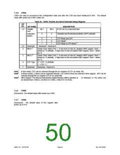
7.3.4 CR03
CR03 can only be accessed in the configuration state and after the CSR has been initialized to 03H. The default
value after power up is 70H (Table 28).
Table 28 - CR03
BIT NO.
BIT NAME
PWRGD
DESCRIPTION
0
Bit 0
0
Pin Function
PWRGD (default)
Reserved
1
1
3
4
5
6
Reserved
Reserved
Reserved
Reserved
Reserved
Reserved- Read as Zero
Reserved - Read as zero
Reserved - Read as one
Reserved - Read as one
Reserved - Read as one
7,2
ADRx/
IRQ_B
Bit - 7 Bit - 2
Pin 92
0
0
1
1
0
1
0
1
Default
Reserved
ADRX
IRQ_B
Note1: See Note2 in section CR05 on page 50.
SMSC DS – SP37E760
Page 49
Rev. 04/13/2001

 SMSC [ SMSC CORPORATION ]