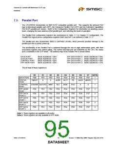
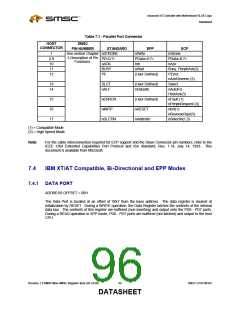
Advanced I/O Controller with Motherboard GLUE Logic
Datasheet
cycle to be performed and the data output to the host CPU, the deassertion of DATASTB latches the
PData for the duration of the read cycle. This register is only available in EPP mode.
7.4.6 EPP DATA PORT 1
ADDRESS OFFSET = 05H
The EPP Data Port 1 is located at an offset of ‘05H’ from the base address. Refer to EPP DATA PORT 0
for a description of operation. This register is only available in EPP mode.
7.4.7 EPP DATA PORT 2
ADDRESS OFFSET = 06H
The EPP Data Port 2 is located at an offset of ‘06H’ from the base address. Refer to EPP DATA PORT 0
for a description of operation. This register is only available in EPP mode.
7.4.8 EPP DATA PORT 3
ADDRESS OFFSET = 07H
The EPP Data Port 3 is located at an offset of ‘07H’ from the base address. Refer to EPP DATA PORT 0
for a description of operation. This register is only available in EPP mode.
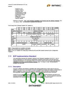
7.5
EPP 1.9 Operation
When the EPP mode is selected in the configuration register, the standard and bi-directional modes are
also available. If no EPP Read, Write or Address cycle is currently executing, then the PDx bus is in the
standard or bi-directional mode, and all output signals (STROBE, AUTOFD, INIT) are as set by the SPP
Control Port and direction is controlled by PCD of the Control port.
In EPP mode, the system timing is closely coupled to the EPP timing. For this reason, a watchdog timer is
required to prevent system lockup. The timer indicates if more than 10usec have elapsed from the start of
the EPP cycle to nWAIT being deasserted (after command). If a time-out occurs, the current EPP cycle is
aborted and the time-out condition is indicated in Status bit 0.
During an EPP cycle, if STROBE is active, it overrides the EPP write signal forcing the PDx bus to always
be in a write mode and the nWRITE signal to always be asserted.
7.5.1 Software Constraints
Before an EPP cycle is executed, the software must ensure that the control register bit PCD is a logic “0”
(i.e., a 04H or 05H should be written to the Control port). If the user leaves PCD as a logic “1”, and
attempts to perform an EPP write, the chip is unable to perform the write (because PCD is a logic “1”) and
will appear to perform an EPP read on the parallel bus, no error is indicated.
SMSC LPC47M182
99
Revision 1.8 SMSC/Non-SMSC Register Sets (02-24-05)
DATASHEET

 SMSC [ SMSC CORPORATION ]