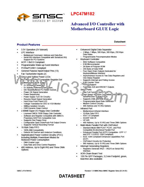
Advanced I/O Controller with Motherboard GLUE Logic
Datasheet
7.6
EPP 1.9 Write
The timing for a write operation (address or data) is shown in timing diagram EPP Write Data or Address
cycle. The chip inserts wait states into the LPC I/O write cycle until it has been determined that the write
cycle can complete. The write cycle can complete under the following circumstances:
1. If the EPP bus is not ready (nWAIT is active low) when nDATASTB or nADDRSTB goes active then
the write can complete when nWAIT goes inactive high.
2. If the EPP bus is ready (nWAIT is inactive high) then the chip must wait for it to go active low before
changing the state of nDATASTB, nWRITE or nADDRSTB. The write can complete once nWAIT is
determined inactive.
Write Sequence of operation
1. The host initiates an I/O write cycle to the selected EPP register.
2. If WAIT is not asserted, the chip must wait until WAIT is asserted.
3. The chip places address or data on PData bus, clears PDIR, and asserts nWRITE.
4. Chip asserts nDATASTB or nADDRSTRB indicating that PData bus contains valid information, and the
WRITE signal is valid.
5. Peripheral deasserts nWAIT, indicating that any setup requirements have been satisfied and the chip
may begin the termination phase of the cycle.
6. a) The chip deasserts nDATASTB or nADDRSTRB, this marks the beginning of the termination phase.
If it has not already done so, the peripheral should latch the information byte now.
b) The chip latches the data from the internal data bus for the PData bus and drives the sync that
indicates that no more wait states are required followed by the TAR to complete the write cycle.
7. Peripheral asserts nWAIT, indicating to the host that any hold time requirements have been satisfied and
acknowledging the termination of the cycle.
8. Chip may modify nWRITE and nPDATA in preparation for the next cycle.
7.7
EPP 1.9 Read
The timing for a read operation (data) is shown in timing diagram EPP Read Data cycle. The chip inserts
wait states into the LPC I/O read cycle until it has been determined that the read cycle can complete. The
read cycle can complete under the following circumstances:
1. If the EPP bus is not ready (nWAIT is active low) when nDATASTB goes active then the read can
complete when nWAIT goes inactive high.
2. If the EPP bus is ready (nWAIT is inactive high) then the chip must wait for it to go active low before
changing the state of nWRITE or before nDATASTB goes active. The read can complete once
nWAIT is determined inactive.
Read Sequence of Operation
1. The host initiates an I/O read cycle to the selected EPP register.
2. If WAIT is not asserted, the chip must wait until WAIT is asserted.
3. The chip tri-states the PData bus and deasserts nWRITE.
4. Chip asserts nDATASTB or nADDRSTRB indicating that PData bus is tri-stated, PDIR is set and the
nWRITE signal is valid.
5. Peripheral drives PData bus valid.
6. Peripheral deasserts nWAIT, indicating that PData is valid and the chip may begin the termination phase
of the cycle.
7. a) The chip latches the data from the PData bus for the internal data bus and deasserts nDATASTB
or nADDRSTRB. This marks the beginning of the termination phase.
b) The chip drives the sync that indicates that no more wait states are required and drives valid data
onto the LAD[3:0] signals, followed by the TAR to complete the read cycle.
8. Peripheral tri-states the PData bus and asserts nWAIT, indicating to the host that the PData bus is tri-
stated.
9. Chip may modify nWRITE, PDIR and nPDATA in preparation for the next cycle.
Revision 1.8 SMSC/Non-SMSC Register Sets (02-24-05)
100
SMSC LPC47M182
DATASHEET

 SMSC [ SMSC CORPORATION ]