Advanced I/O Controller with Motherboard GLUE Logic
Datasheet
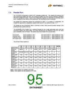
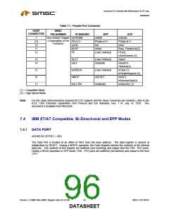
Table 7.1 - Parallel Port Connector
SMSC
PIN NUMBER
HOST
CONNECTOR
STANDARD
EPP
ECP
1
See section Chapter nSTROBE
nWrite
nStrobe
3 Description of Pin
Functions.
2-9
10
11
12
PD<0:7>
nACK
BUSY
PE
PData<0:7>
PData<0:7>
Intr
nWait
nAck
Busy, PeriphAck(3)
PError,
(User Defined)
nAckReverse (3)
Select
nAutoFd,
13
14
SLCT
nALF
(User Defined)
nDatastb
HostAck(3)
nFault (1)
nPeriphRequest (3)
nInit(1)
nReverseRqst(3)
nSelectIn(1,3)
15
16
17
nERROR
nINITP
(User Defined)
nRESET
nSLCTIN
nAddrstrb
(1) = Compatible Mode
(3) = High Speed Mode
Note:
For the cable interconnection required for ECP support and the Slave Connector pin numbers, refer to the
IEEE 1284 Extended Capabilities Port Protocol and ISA Standard, Rev. 1.14, July 14, 1993. This
document is available from Microsoft.
7.4
IBM XT/AT Compatible, Bi-Directional and EPP Modes
7.4.1 DATA PORT
ADDRESS OFFSET = 00H
The Data Port is located at an offset of ‘00H’ from the base address. The data register is cleared at
initialization by RESET. During a WRITE operation, the Data Register latches the contents of the internal
data bus. The contents of this register are buffered (non inverting) and output onto the PD0 - PD7 ports.
During a READ operation in SPP mode, PD0 - PD7 ports are buffered (not latched) and output to the host
CPU.
Revision 1.8 SMSC/Non-SMSC Register Sets (02-24-05)
96
SMSC LPC47M182
DATASHEET

 SMSC [ SMSC CORPORATION ]