Advanced I/O Controller with Motherboard GLUE Logic
Datasheet
BIT 6 LOW POWER
A logic “1” written to this bit will put the floppy controller into manual low power mode. The floppy
controller clock and data separator circuits will be turned off. The controller will come out of manual low
power mode after a software reset or access to the Data Register or Main Status Register.
BIT 7 SOFTWARE RESET
This active high bit has the same function as the DOR RESET (DOR bit 2) except that this bit is self
clearing.
Separator circuits will be turned off. The controller will come out of manual low power.
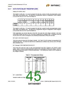
Note: The DSR is Shadowed in the Floppy Data Rate Select Shadow Register, located at the offset 0x19 in the
Power Control Logical Device (when LD_NUM=0) or Runtime Register Block Logical Device (when LD_NUM=1).
Table 6.8 - Data Rates
DRIVE RATE
DATA RATE
DATA RATE
DRATE(1)
DENSEL
DRT1
DRT0
SEL1
SEL0
MFM
FM
1
0
0
0
0
0
0
0
0
0
1
0
0
1
1
0
1
0
1Meg
500
300
---
1
1
0
0
1
0
0
1
1
0
1
0
250
150
125
250
0
0
0
0
1
1
1
1
1
0
0
1
1
0
1
0
1Meg
500
500
---
1
1
0
0
1
0
0
1
1
0
1
0
250
250
125
250
1
1
1
1
0
0
0
0
1
0
0
1
1
0
1
0
1Meg
500
2Meg
---
250
---
1
1
0
0
1
0
0
1
1
0
1
0
250
125
Drive Rate Table (Recommended) 00 = 360K, 1.2M, 720K, 1.44M and 2.88M Vertical Format
01 = 3-Mode Drive
10 = 2 Meg Tape
Note 1: The DRATE and DENSEL values are mapped onto the DRVDEN pins.
Table 6.9 - DRVDEN Mapping
DT1
0
DT0
0
DRVDEN1 (1)
DRVDEN0 (1)
DRIVE TYPE
4/2/1 MB 3.5”
2/1 MB 5.25” FDDS
DRATE0
DENSEL
2/1.6/1 MB 3.5” (3-MODE)
1
0
1
0
1
1
DRATE0
DRATE0
DRATE1
DRATE1
nDENSEL
DRATE0
PS/2
Revision 1.8 SMSC/Non-SMSC Register Sets (02-24-05)
46
SMSC LPC47M182
DATASHEET

 SMSC [ SMSC CORPORATION ]