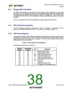
Advanced I/O Controller with Motherboard GLUE Logic
Datasheet
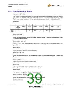
BIT 1 nDRIVE SELECT 3
The DS3 disk interface is not supported.
BIT 2 WRITE GATE
Active high status of the latched WGATE output signal. This bit is latched by the active going edge of
WGATE and is cleared by the read of the DIR register.
BIT 3 READ DATA
Active high status of the latched RDATA output signal. This bit is latched by the inactive going edge of
RDATA and is cleared by the read of the DIR register.
BIT 4 WRITE DATA
Active high status of the latched WDATA output signal. This bit is latched by the inactive going edge of
WDATA and is cleared by the read of the DIR register. This bit is not gated with WGATE.
BIT 5 nDRIVE SELECT 0
Active low status of the DS0 disk interface output.
BIT 6 nDRIVE SELECT 1
Active low status of the DS1 disk interface output.
BIT 7 nDRV2
Active low status of the DRV2 disk interface input. Note: This function is not supported.
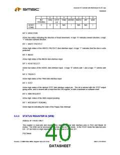
6.4.5 DIGITAL OUTPUT REGISTER (DOR)
Address 3F2 READ/WRITE
The DOR controls the drive select and motor enables of the disk interface outputs. It also contains the
enable for the DMA logic and a software reset bit. The contents of the DOR are unaffected by a software
reset. The DOR can be written to at any time.
7
6
5
4
3
2
1
0
MOT
MOT
MOT
MOT
DMAEN
nRESET
DRIVE
DRIVE
EN3
EN2
EN1
EN0
SEL1
SEL0
RESET
COND.
0
0
0
0
0
0
0
0
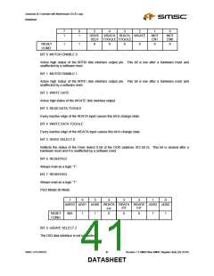
BIT 0 and 1 DRIVE SELECT
These two bits are binary encoded for the drive selects, thereby allowing only one drive to be selected at
one time.
BIT 2 nRESET
Revision 1.8 SMSC/Non-SMSC Register Sets (02-24-05)
42
SMSC LPC47M182
DATASHEET

 SMSC [ SMSC CORPORATION ]