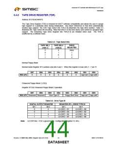
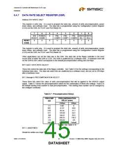
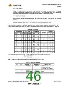
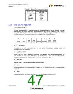
Advanced I/O Controller with Motherboard GLUE Logic
Datasheet
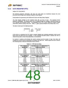
6.4.9 DATA REGISTER (FIFO)
Address 3F5 READ/WRITE
All command parameter information, disk data and result status are transferred between the host
processor and the floppy disk controller through the Data Register.
Data transfers are governed by the RQM and DIO bits in the Main Status Register.
The Data Register defaults to FIFO disabled mode after any form of reset. This maintains PC/AT
hardware compatibility. The default values can be changed through the Configure command (enable full
FIFO operation with threshold control). The advantage of the FIFO is that it allows the system a larger
DMA latency without causing a disk error. Table 6.11 gives several examples of the delays with a FIFO.
The data is based upon the following formula:
Threshold #
x
1
x 8 - 1.5 us =
DELAY
DATA
RATE
At the start of a command, the FIFO action is always disabled and command parameters must be sent
based upon the RQM and DIO bit settings. As the command execution phase is entered, the FIFO is
cleared of any data to ensure that invalid data is not transferred.
An overrun or underrun will terminate the current command and the transfer of data. Disk writes will
complete the current sector by generating a 00 pattern and valid CRC. Reads require the host to remove
the remaining data so that the result phase may be entered.
Table 6.11 - FIFO Service Delay
FIFO THRESHOLD
EXAMPLES
MAXIMUM DELAY TO SERVICING AT
2 Mbps DATA RATE
1 x 4 us - 1.5 us = 2.5 us
2 x 4 us - 1.5 us = 6.5 us
8 x 4 us - 1.5 us = 30.5 us
15 x 4 us - 1.5 us = 58.5 us
1 byte
2 bytes
8 bytes
15 bytes
FIFO THRESHOLD
EXAMPLES
MAXIMUM DELAY TO SERVICING AT
1 Mbps DATA RATE
1 x 8 us - 1.5 us = 6.5 us
2 x 8 us - 1.5 us = 14.5 us
8 x 8 us - 1.5 us = 62.5 us
15 x 8 us - 1.5 us = 118.5 us
1 byte
2 bytes
8 bytes
15 bytes
FIFO THRESHOLD
EXAMPLES
MAXIMUM DELAY TO SERVICING AT
500 Kbps DATA RATE
1 x 16 us - 1.5 us = 14.5 us
2 x 16 us - 1.5 us = 30.5 us
8 x 16 us - 1.5 us = 126.5 us
15 x 16 us - 1.5 us = 238.5 us
1 byte
2 bytes
8 bytes
15 bytes
Revision 1.8 SMSC/Non-SMSC Register Sets (02-24-05)
48
SMSC LPC47M182
DATASHEET

 SMSC [ SMSC CORPORATION ]