Advanced I/O Controller with Motherboard GLUE Logic
Datasheet
A logic “0” written to this bit resets the Floppy disk controller. This reset will remain active until a logic “1”
is written to this bit. This software reset does not affect the DSR and CCR registers, nor does it affect the
other bits of the DOR register. The minimum reset duration required is 100ns, therefore toggling this bit by
consecutive writes to this register is a valid method of issuing a software reset.
BIT 3 DMAEN
PC/AT and Model 30 Mode:
Writing this bit to logic “1” will enable the DMA and interrupt functions. This bit being a logic “0” will disable
the DMA and interrupt functions. This bit is a logic “0” after a reset and in these modes.
PS/2 Mode: In this mode the DMA and interrupt functions are always enabled. During a reset, this bit will
be cleared to a logic “0”.
BIT 4 MOTOR ENABLE 0
This bit controls the MTR0 disk interface output. A logic “1” in this bit will cause the output pin to go active.
BIT 5 MOTOR ENABLE 1
This bit controls the MTR1 disk interface output. A logic “1” in this bit will cause the output pin to go active.
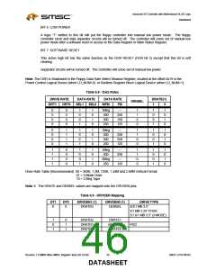
DRIVE
DOR VALUE
1CH
0
1
2DH
Table 6.3 - Internal 2 Drive Decode – Normal
DIGITAL OUTPUT
DRIVE SELECT OUTPUTS
(ACTIVE LOW)
MOTOR ON OUTPUTS
(ACTIVE LOW)
REGISTER
Bit 5 Bit 4 Bit1 Bit 0
nDS1
nDS0
nMTR1
nMTR0
nBIT 4
nBIT 4
nBIT 4
X
1
0
1
X
0
0
0
X
0
1
X
1
0
1
0
1
1
nBIT 5
nBIT 5
nBIT 5
Table 6.4 - Internal 2 Drive Decode – Drives 0 and 1 Swapped
DIGITAL OUTPUT
REGISTER
Bit 5 Bit 4 Bit1 Bit 0
DRIVE SELECT OUTPUTS
(ACTIVE LOW)
MOTOR ON OUTPUTS
(ACTIVE LOW)
nDS1
nDS0
nMTR1
nBIT 4
nBIT 4
nBIT 4
nMTR0
nBIT 5
nBIT 5
nBIT 5
X
1
0
1
X
0
0
0
X
0
1
X
0
1
1
1
0
1
BIT 6 MOTOR ENABLE 2
The MTR2 disk interface output is not supported in the LPC47M182.
BIT 7 MOTOR ENABLE 3
The MTR3 disk interface output is not supported in the LPC47M182.
SMSC LPC47M182
43
Revision 1.8 SMSC/Non-SMSC Register Sets (02-24-05)
DATASHEET

 SMSC [ SMSC CORPORATION ]