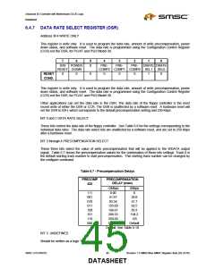
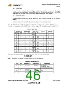
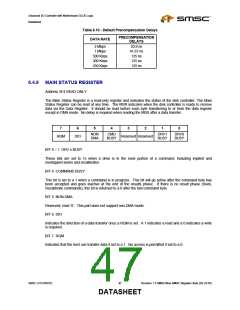
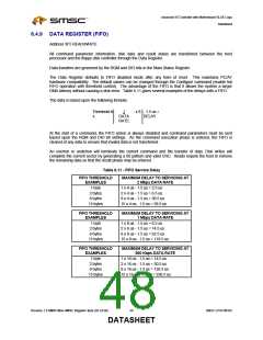
Advanced I/O Controller with Motherboard GLUE Logic
Datasheet
6.4.10 DIGITAL INPUT REGISTER (DIR)
Address 3F7 READ ONLY
This register is read-only in all modes.
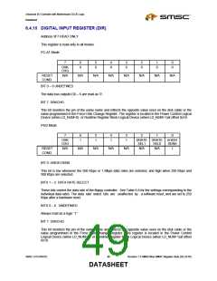
PC-AT Mode
7
6
0
5
0
4
0
3
0
2
0
1
0
0
0
DSK
CHG
RESET
COND.
N/A
N/A
N/A
N/A
N/A
N/A
N/A
N/A
BIT 0 – 6 UNDEFINED
The data bus outputs D0 – 6 are read as ‘0’.
BIT 7 DSKCHG
This bit monitors the pin of the same name and reflects the opposite value seen on the disk cable or the
value programmed in the Force Disk Change Register. The register is located in the Power Control Logical
Device (when LD_NUM=0) or Runtime Register Block Logical Device (when LD_NUM=1)at offset 0x18.
PS/2 Mode
7
6
1
5
1
4
1
3
1
2
1
0
DSK
DRATE DRATE
nHIGH
CHG
SEL1
N/A
SEL0
N/A
DENS
RESET
COND.
N/A
N/A
N/A
N/A
N/A
1
BIT 0 nHIGH DENS
This bit is low whenever the 500 Kbps or 1 Mbps data rates are selected, and high when 250 Kbps and
300 Kbps are selected.
BITS 1 – 2 DATA RATE SELECT
These bits control the data rate of the floppy controller. See Table 6.8 for the settings corresponding to the
individual data rates. The data rate select bits are unaffected by a software reset, and are set to 250
Kbps after a hardware reset.
BITS 3 – 6 UNDEFINED
Always read as a logic “1”
BIT 7 DSKCHG
This bit monitors the pin of the same name and reflects the opposite value seen on the disk cable or the
value programmed in the Force Disk Change Register. This register is located in the Power Control
Logical Device (when LD_NUM=0) or Runtime Register Block Logical Device (when LD_NUM=1)at offset
0x18.
SMSC LPC47M182
49
Revision 1.8 SMSC/Non-SMSC Register Sets (02-24-05)
DATASHEET

 SMSC [ SMSC CORPORATION ]