Advanced I/O Controller with Motherboard GLUE Logic
Datasheet
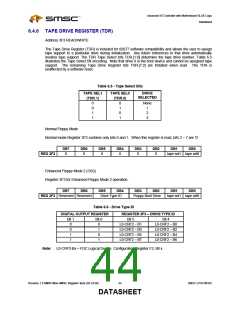
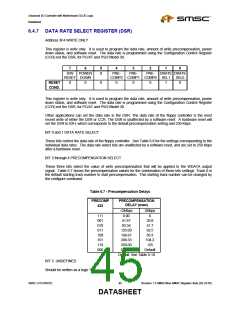
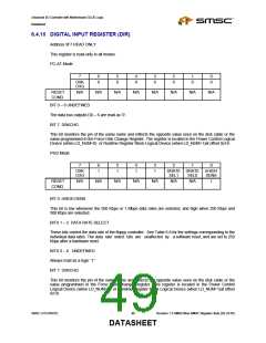
6.4.7 DATA RATE SELECT REGISTER (DSR)
Address 3F4 WRITE ONLY
This register is write only. It is used to program the data rate, amount of write precompensation, power
down status, and software reset. The data rate is programmed using the Configuration Control Register
(CCR) not the DSR, for PC/AT and PS/2 Model 30.
7
6
5
0
4
3
2
1
0
S/W
POWER
PRE-
PRE-
PRE-
DRATE DRATE
RESET DOWN
COMP2 COMP1 COMP0 SEL1
SEL0
0
RESET
COND.
0
0
0
0
0
0
1
This register is write only. It is used to program the data rate, amount of write precompensation, power
down status, and software reset. The data rate is programmed using the Configuration Control Register
(CCR) not the DSR, for PC/AT and PS/2 Model 30.
Other applications can set the data rate in the DSR. The data rate of the floppy controller is the most
recent write of either the DSR or CCR. The DSR is unaffected by a software reset. A hardware reset will
set the DSR to 02H, which corresponds to the default precompensation setting and 250 Kbps.
BIT 0 and 1 DATA RATE SELECT
These bits control the data rate of the floppy controller. See Table 6.8 for the settings corresponding to the
individual data rates. The data rate select bits are unaffected by a software reset, and are set to 250 Kbps
after a hardware reset.
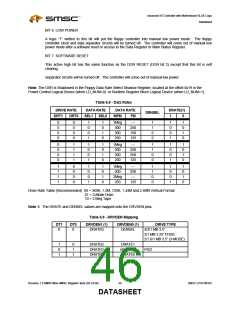
BIT 2 through 4 PRECOMPENSATION SELECT
These three bits select the value of write precompensation that will be applied to the WDATA output
signal. Table 6.7 shows the precompensation values for the combination of these bits settings. Track 0 is
the default starting track number to start precompensation. This starting track number can be changed by
the configure command.
Table 6.7 - Precompensation Delays
PRECOMP
432
PRECOMPENSATION
DELAY (nsec)
<2Mbps
0.00
2Mbps
0
111
001
010
011
100
101
110
000
41.67
20.8
41.7
62.5
83.3
104.2
125
83.34
125.00
166.67
208.33
250.00
Default
Default
Default: See Table 6.10
BIT 5 UNDEFINED
Should be written as a logic “0”.
SMSC LPC47M182
45
Revision 1.8 SMSC/Non-SMSC Register Sets (02-24-05)
DATASHEET

 SMSC [ SMSC CORPORATION ]