Advanced I/O Controller with Motherboard GLUE Logic
Datasheet
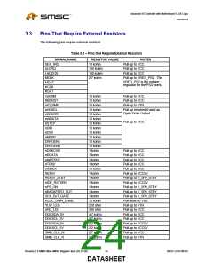
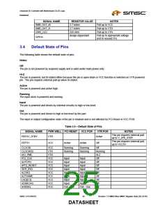
SIGNAL NAME
SMB_DAT_M
SMB_DAT_R
RESISTOR VALUE
2.7 kohm
2.7 kohm
NOTES
Pull-up to VCC
Pull-up to VTR
GRN_LED
220 ohm
design-dependant
Pull-up to VTR
Pull-up to appropriate voltage
(not to exceed 5V)
GPIOs
3.4
Default State of Pins
The following table shows the default state of pins.
Notes:
Off
The pin is not powered by suspend supply and is valid under main power only.
Hi-Z
The pin is powered, but tri-stated either because the pin is open-drain or VCC function is selected on VTR powered
pin. The pin requires external pull-up when tri-stated.
Active
The pin is powered and active high.
Running
The input clock is powered and running.
Input
The pin is powered and driven by external circuitry to high or low level.
Out
The pin is powered and driven to high or low level by the part.
The input or output configuration state of the pin is retained and is not affected by PCI Reset or VCC POR.
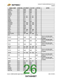
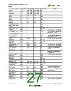
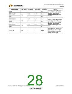
Table 3.4 – Default State of Pins
SIGNAL NAME
PWR WELL PCI RESET
VCC POR
VTR POR
NOTES
This pin requires external pull-
REF5V_STBY
VTR
-
-
Active
up to V_5P0_STBY
This pin requires external pull-
up to VCC5V
REF5V
VCC
Active
Active
Off
CLOCKI
VCC
VTR
VTR
VCC
VCC
VCC
VCC
VCC
VCC
VCC
VCC
VCC
Running
Running
-
Input
Input
Input
Input
Input
Input
Running
Running
-
Input
Input
Input
Input
Input
Input
Off
CLOCKI32
nIO_PME
PCI_CLK
nLPCPD
nPCI_RESET
SER_IRQ
nLDRQ
nLFRAME
LAD[0:3]
nDSKCHG
Running
Hi-Z
Off
Off
Off
Off
Off
Off
Off
Input
Input
Out – low
Input
Input
Out – low
Off
Off
nHDSEL
SMSC LPC47M182
25
Revision 1.8 SMSC/Non-SMSC Register Sets (02-24-05)
DATASHEET

 SMSC [ SMSC CORPORATION ]