Advanced I/O Controller with Motherboard GLUE Logic
Datasheet
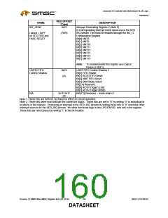
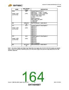
REG OFFSET
(Type)
NAME
DESCRIPTION
GP24
0x0C
General Purpose I/O bit 2.4
Bit[0] In/Out : =1 Input, =0 Output
Bit[1] Polarity : =1 Invert, =0 No Invert
Bit[2] Alternate Function Select
1=nCDC_DWN_ENAB
0=GPIO
Default = 0x05
on VTR POR
(R/W)
Bits[6:3] Reserved
Bit[7] Output Type Select
1=Open Drain
0=Push Pull
N/A
0x0D-0x14
(R)
Bits[7:0] Reserved – reads return 0
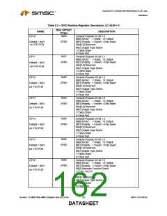
GP1
0x15
General Purpose I/O Data Register 1
Bit[0] GP10
Default = 0x00
on VTR POR
(R/W)
Bit[1] GP11
Bit[2] GP12
Bit[3] GP13
Bit[4] GP14
Bit[5] GP15
Bit[6] GP16
Bit[7] GP17
GP2
0x16
General Purpose I/O Data Register 2
Bit[0] GP20
Default = 0x00
on VTR POR
(R/W)
Bit[1] GP21
Bit[2] GP22
Bit[3] GP23
Bit[4] GP24
Bits[7:5] Reserved
Bits[7:0] Reserved – reads return 0
N/A
0x17-0x1F
(R)
Note 1: The In/Out, Polarity and Output Type Select Bits do not apply when DDCSCL/DDCSDA signals are selected.
Note 2: If the EETI function is selected for this GPIO then both a high-to-low and low-to-high edge will set the PME
and MSC status bits.
Revision 1.8 SMSC/Non-SMSC Register Sets (02-24-05)
164
SMSC LPC47M182
DATASHEET

 SMSC [ SMSC CORPORATION ]