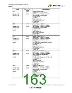
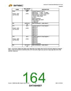
Advanced I/O Controller with Motherboard GLUE Logic
Datasheet
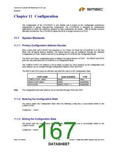
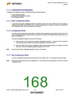
Chapter 11 Configuration
The Configuration of the LPC47M182 is very flexible and is based on the configuration architecture
implemented in typical Plug-and-Play components. The LPC47M182 is designed for motherboard
applications in which the resources required by their components are known. With its flexible resource
allocation architecture, the LPC47M182 allows the BIOS to assign resources at POST.
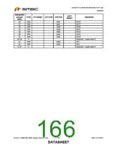
11.1 System Elements
11.1.1 Primary Configuration Address Decoder
After a hard reset (nPCI_RESET pin asserted) or Vcc Power On Reset the LPC47M182 is in the Run
Mode with all logical devices disabled. The logical devices may be configured through two standard
Configuration I/O Ports (INDEX and DATA) by placing the LPC47M182 into Configuration Mode.
The BIOS uses these configuration ports to initialize the logical devices at POST. The INDEX and DATA
ports are only valid when the LPC47M182 is in Configuration Mode.
The CONFIG PORT’s I/O address is set to 0x02E at power-up. Once powered up the configuration port
base address can be changed through configuration registers CR26 and CR27.
The INDEX and DATA ports are effective only when the chip is in the Configuration State.
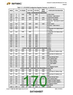
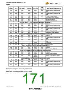
PORT NAME
CONFIG PORT (Note)
INDEX PORT (Note)
DATA PORT
BASE ADDRESS
0x02E
0x02E
TYPE
Write
Read/Write
Read/Write
INDEX PORT + 1
Note:
The configuration port base address can be relocated through CR26 and CR27.
11.1.2 Entering the Configuration State
The device enters the Configuration State when the following Config Key is successfully written to the
CONFIG PORT.
Config Key = <0x55>
11.1.3 Exiting the Configuration State
The device exits the Configuration State when the following Config Key is successfully written to the
CONFIG PORT.
Config Key = <0xAA>
SMSC LPC47M182
167
Revision 1.8 SMSC/Non-SMSC Register Sets (02-24-05)
DATASHEET

 SMSC [ SMSC CORPORATION ]