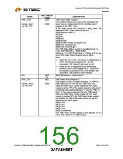
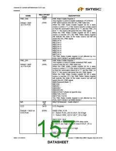
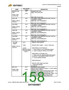
Advanced I/O Controller with Motherboard GLUE Logic
Datasheet
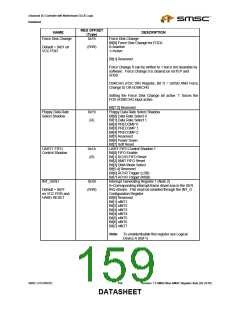
REG OFFSET
(Type)
NAME
INT_GEN2
DESCRIPTION
0x1C
Interrupt Generating Register 2 (Note 2)
0=Corresponding Interrupt frame driven low in the SER
Default = 0xFF
on VCC POR and
HARD RESET
(R/W)
IRQ stream. This must be enabled through the INT_G
Configuration Register.
Bit[0] nINT8
Bit[1] nINT9
Bit[2] nINT10
Bit[3] nINT11
Bit[4] nINT12
Bit[5] nINT13
Bit[6] nINT14
Bit[7] nINT15
Note: To enable/disable this register see Logical
Device A (0xF1)
UART2 FIFO
0x1D
(R)
UART FIFO Control Shadow 2
Bit[0] FIFO Enable
Control Shadow
Bit[1] RCVR FIFO Reset
Bit[2] XMIT FIFO Reset
Bit[3] DMA Mode Select
Bit[5:4] Reserved
Bit[6] RCVR Trigger (LSB)
Bit[7] RCVR Trigger (MSB)
Bits[7:0] Reserved – reads return 0
N/A
0x1E-0x1F
(R)
Note 1: These bits are R/W bit, but have no effect on circuit operation.
Note 2: These bits when read indicate the current bit status. These bits are set to “0” by writing “0” to individual bit
locations in this register. Producing an interrupt in the SER_IRQ stream by setting these bits to “0” overrides other
interrupt sources for the SER_IRQ stream. No other functional logic in the LPC47M182 sets bits in the register.
These bits are only cleared by writing “1” to the bit location.
Revision 1.8 SMSC/Non-SMSC Register Sets (02-24-05)
160
SMSC LPC47M182
DATASHEET

 SMSC [ SMSC CORPORATION ]