Advanced I/O Controller with Motherboard GLUE Logic
Datasheet
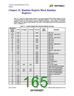
Chapter 10 Runtime Register Block Runtime
Registers
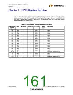
Table 10.1 shows the runtime register summary. The Runtime Register Block runtime registers can only
be accessed when LD_NUM bit in the TEST 7 configuration register is ‘1’. See “Power Control Runtime
Registers” section and “GPIO Runtime Registers” section for description of these registers. Note these
offsets replace the register offsets defined in the Power Control logical device and GPIO logical device
when LD_NUM bit is ‘1’
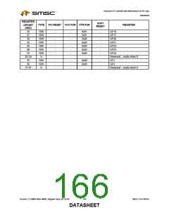
Table 10.1 – Runtime Register Block Runtime Registers Summary
REGISTER
SOFT
TYPE
PCI RESET VCC POR VTR POR
REGISTER
OFFSET
RESET
(HEX)
00
01-03
04
05-07
08
R/W
R
R/W
R
R/W
R/W
R/W
R
R/W
R/W
R/W
R
R/W
R/W
R
R
R
-
-
-
-
-
-
-
-
-
-
-
-
-
-
-
-
-
-
-
-
-
-
-
-
-
-
-
-
-
-
-
-
0x00
-
0x00
-
0x00
0x00
0x00
-
0x00
0x00
0x00
-
0x03
0x00
0x00
0x00
0x00
0x00
0x80
0x00
-
-
-
-
-
-
-
-
-
-
-
-
-
-
-
-
-
-
-
-
-
-
-
-
-
-
-
-
-
-
-
-
-
-
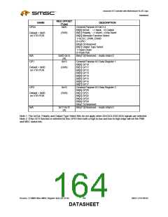
PME_STS
Reserved – reads return 0
PME_EN
Reserved – reads return 0
PME_STS3
PME_STS2
PME_STS1
Reserved – reads return 0
PME_EN3
PME_EN2
PME_EN1
Reserved – reads return 0
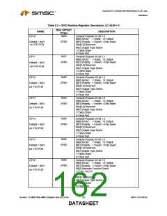
LED
Keyboard Scan Code
Tach1 LSB
Tach1 MSB
Tach2 LSB
Tach2 MSB
nIO_PME Register
MSC_STS
Force Disk Change
Floppy Data Rate Select Shadow
UART1 FIFO Control Shadow
Interrupt Generating Register 1
Interrupt Generating Register 2
UART2 FIFO Control Shadow
Reserved – reads return 0
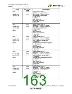
GP10
GP11
GP12
GP13
GP14
09
0A
0B
0C
0D
0E
0F
10
11
12
13
14
-
-
-
-
-
-
-
-
15
16
17
18
R
R/W
R/W
R/W
R
0x01
-
-
0xFF
0xFF
-
-
-
-
-
-
-
-
0x01
-
-
0xFF
0xFF
-
-
-
-
-
-
-
-
19
-
-
-
-
-
-
1A
1B
1C
1D
1F
20
21
22
23
24
R
R/W
R/W
R
R
R/W
R/W
R/W
R/W
R/W
R/W
0x01
0x01
0x01
0x01
0x01
0x01
25
GP15
SMSC LPC47M182
165
Revision 1.8 SMSC/Non-SMSC Register Sets (02-24-05)
DATASHEET

 SMSC [ SMSC CORPORATION ]