Advanced I/O Controller with Motherboard GLUE Logic
Datasheet
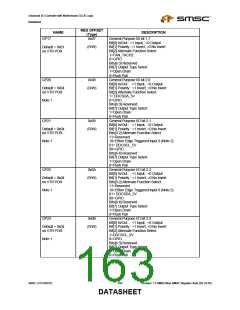
REG OFFSET
NAME
DESCRIPTION
(Type)
GP17
0x07
General Purpose I/0 bit 1.7
Bit[0] In/Out : =1 Input, =0 Output
Bit[1] Polarity :=1 Invert, =0 No Invert
Bit[2] Alternate Function Select
1=FAN_TACH2
Default = 0x01
on VTR POR
(R/W)
0=GPIO
Bits[6:3] Reserved
Bit[7] Output Type Select
1=Open Drain
0=Push Pull
GP20
0x08
General Purpose I/0 bit 2.0
Bit[0] In/Out : =1 Input, =0 Output
Bit[1] Polarity : =1 Invert, =0 No Invert
Bit[2] Alternate Function Select
1= DDCSDA_5V
Default = 0x04
on VTR POR
(R/W)
Note 1
GP21
0=GPIO
Bits[6:3] Reserved
Bit[7] Output Type Select
1=Open Drain
0=Push Pull
0x09
General Purpose I/O bit 2.1
Bit[0] In/Out : =1 Input, =0 Output
Bit[1] Polarity : =1 Invert, =0 No Invert
Bits[3:2] Alternate Function Select
11=Reserved
Default = 0x04
on VTR POR
(R/W)
Note 1
10=Either Edge Triggered Input 0 (Note 2)
01= DDCSCL_5V
00=GPIO
Bits[6:4] Reserved
Bit[7] Output Type Select
1=Open Drain
0=Push Pull
GP22
0x0A
General Purpose I/O bit 2.2
Bit[0] In/Out : =1 Input, =0 Output
Bit[1] Polarity : =1 Invert, =0 No Invert
Bits[3:2] Alternate Function Select
11=Reserved
Default = 0x04
on VTR POR
(R/W)
Note 1
10=Either Edge Triggered Input 0 (Note 2)
01= DDCSDA_3V
00=GPIO
Bits[6:4] Reserved
Bit[7] Output Type Select
1=Open Drain
0=Push Pull
GP23
0x0B
General Purpose I/O bit 2.3
Bit[0] In/Out : =1 Input, =0 Output
Bit[1] Polarity : =1 Invert, =0 No Invert
Bit[2] Alternate Function Select
1=DDCSCL_3V
Default = 0x04
on VTR POR
(R/W)
Note 1
0=GPIO
Bits[6:3] Reserved
Bit[7] Output Type Select
1=Open Drain
0=Push Pull
SMSC LPC47M182
163
Revision 1.8 SMSC/Non-SMSC Register Sets (02-24-05)
DATASHEET

 SMSC [ SMSC CORPORATION ]