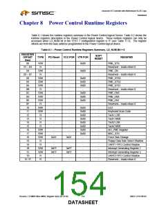
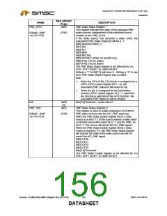
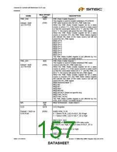
Advanced I/O Controller with Motherboard GLUE Logic
Datasheet
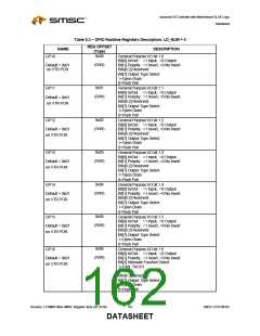
REG OFFSET
(Type)
NAME
DESCRIPTION
Keyboard Scan
Code
0x11
Keyboard Scan Code
Bit[0] LSB of Scan Code
(R/W)
. . .
Default = 0x00
on VTR POR
. . .
. . .
Bit[7] MSB of Scan Code
This register is least significant 8-bit of the 16-bit Fan
Tachometer 1 reading.
Tach1 LSB
0x12
(R)
Default = 0x00 on
VTR POR
Bit[0] FAN_TACH1 Reading Bit 0
…
Bit[7] FAN_TACH1 Reading Bit 7
This register is most significant 8-bit of the 16-bit Fan
Tachometer 1 reading.
Tach1 MSB
0x13
(R)
Default = 0x00 on
VTR POR
Bit[0] FAN_TACH1 Reading Bit 8
…
Bit[7] FAN_TACH1 Reading Bit 15
This register is least significant 8-bit of the 16-bit Fan
Tachometer 2 reading.
Tach2 LSB
0x14
(R)
Default = 0x00 on
VTR POR
Bit[0] FAN_TACH2 Reading Bit 0
…
Bit[7] FAN_TACH2 Reading Bit 7
This register is most significant 8-bit of the 16-bit Fan
Tachometer 2 reading.
Tach2 MSB
0x15
(R)
Default = 0x00 on
VTR POR
Bit[0] FAN_TACH2 Reading Bit 8
…
Bit[7] FAN_TACH2 Reading Bit 15
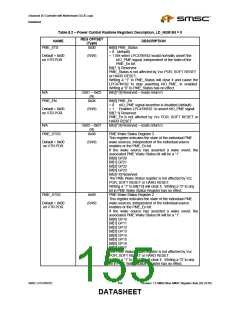
nIO_PME
Register
0x16
Bit[0] nIO_PME Reserved
(R/W)
Bit[1]nIO_PME Polarity : =1 Invert, =0 No Invert
Default = 0x84 on
VTR POR
except
Bit[2] PWRGD_PLATFORM_SEL
1 = select PWRGD_PLATFORM delay (default)
0 = select no delay for PWRGD_PLATFORM
Bits[3:2] are Read
Only when Bit[3]
set to ‘1’
Bit[3] PWRGD_PLAFORM LOCK
1 = When set to one, Bit[2] and Bit[3] of this register
become RO. They remain RO until a VTR POR.
0 = no lock operation (Default)
Bits[6:4] Reserved
Bit[7] nIO_PME Output Type Select
1=Open Drain (default)
0=Push Pull
MSC_STS
0x17
Miscellaneous Status Register
Bits[1:0] can be cleared by writing a 1 to their position
(writing a 0 has no effect).
Bit[0] Either Edge Triggered Interrupt Input 0 Status. This
bit is set when an edge occurs on the GP21 pin.
Bit[1] Either Edge Triggered Interrupt Input 1 Status. This
bit is set when an edge occurs on the GP22 pin.
Bit[7:2] Reserved. This bit always returns zero.
Default = 0x00
on VTR POR
(R/W)
Revision 1.8 SMSC/Non-SMSC Register Sets (02-24-05)
158
SMSC LPC47M182
DATASHEET

 SMSC [ SMSC CORPORATION ]