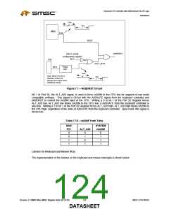
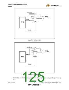
Advanced I/O Controller with Motherboard GLUE Logic
Datasheet
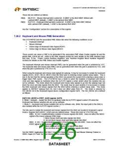
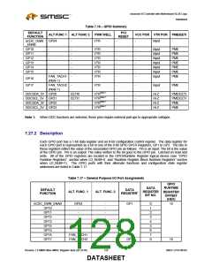
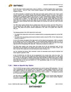
Table 7.16 – GPIO Summary
PCI
DEFAULT
ALT FUNC 1 ALT FUNC 2
PWR WELL
VCC POR VTR POR PME/EETI
FUNCTION
RESET
nCDC_DWN
GP24
-
VTR
-
-
Input
-
_ENAB
GP10
GP11
GP12
GP13
GP14
GP15
-
-
-
-
-
-
-
-
-
-
-
-
-
VTR
VTR
VTR
VTR
VTR
VTR
VTR
-
-
-
-
-
-
-
-
-
-
-
-
-
-
Input
Input
Input
Input
Input
Input
Input
PME
PME
PME
PME
PME
PME
PME
FAN_TACH1
(Note 1)
FAN_TACH2
(Note 1)
GP16
GP17
-
VTR
-
-
Input
PME
DDCSDA_5V GP20
DDCSCL_5V GP21
DDCSDA_3V GP22
DDCSCL_3V GP23
EETI0
EETI1
-
-
VTRNote 1
VTRNote 1
VTRNote 1
VTRNote 1
-
-
-
-
-
-
-
-
Hi-Z
Hi-Z
Hi-Z
Hi-Z
PME/EETI
PME/EETI
PME
PME
Note 1: When DDC functions are selected, these pins require external pull-ups to appropriate voltages.
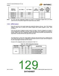
7.27.2 Description
Each GPIO port has a 1-bit data register and an 8-bit configuration control register. The data register for
each GPIO port is represented as a bit in one of the 8-bit GPIO DATA Registers, GP1 to GP2. The bits in
these registers reflect the value of the associated GPIO pin as follows. Pin is an input: The bit is the value
of the GPIO pin. Pin is an output: The value written to the bit goes to the GPIO pin. Latched on read and
write. All of the GPIO registers are located in the GPIO/Runtime Register logical device (see “GPIO
Runtime Registers” section when LD_NUM=0 and “Runtime Register Block Runtime Registers” section
when LD_NUM=1). The GPIO ports with their alternate functions and configuration state register
addresses are listed in Table 7.17.
Table 7.17 – General Purpose I/O Port Assignments
GPIO
RUNTIME
DATA
REGISTER
BIT NO.
DEFAULT
DATA
ALT. FUNC. 1
ALT. FUNC. 2
FUNCTION
REGISTER1
REGISTER
OFFSET
(HEX)
nCDC_DWN_ENAB
GP10
GP24
-
-
-
-
-
-
-
-
-
-
-
-
-
-
-
GP1
0
1
2
3
4
5
6
7
0
15
GP11
GP12
GP13
GP14
GP15
GP16
GP17
FAN_TACH1
FAN_TACH2
GP2
16
Revision 1.8 SMSC/Non-SMSC Register Sets (02-24-05)
128
SMSC LPC47M182
DATASHEET

 SMSC [ SMSC CORPORATION ]