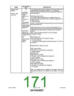
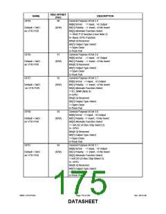
REG OFFSET
(hex)
NAME
DESCRIPTION
Device Disable
Register
22
If “0” (enabled), bits[7:3] have no effect on the devices; devices are
controlled by their respective activate bits. If “1” (disabled),
bits[7:3] override the activate bits in the configuration registers for
each logical block.
Read/Write
when GP43
register
bits[3:2] = 01
AND
GP43 pin = 0
OR
Default = 0x00
VTR POR
Bit[0] Floppy Write Protect.
0= no effect: floppy write protection is controlled by the write
protect pin or the Forced Write Protect bit (bit 0 of register 0xF1 in
Logical Device 0);
1= Write Protected.
GP43 register
bits[3:2] ≠ 01
(Device Disable
Register Bit[1]
must be 0)
If set to 1, this bit overrides the write protect pin on the part and the
forced write protect bit.
nWRTPRT (to the FDC Core) = WP (FDC SRA Register, Bit 1) =
(Floppy Write Protect) OR nWRTPRT(from the FDD Interface) OR
(nDS0 AND Force Write Protect ) OR (nDS1 AND Force Write
Protect ).
READ-ONLY
When GP43
register bits[3:2]
=01 AND GP43
pin = 1
Note: The Force Write Protect bit is in the FDD Option
Configuration register.
Bit[1] Register Lock
OR
This bit is cleared on VCC POR and PCI Reset.
0 - No effect (Default)
Device Disable
Register
1 - All of the bits in this register are Read Only until a VCC POR or
PCI RESET.
Bit[1]=1
Bits[2] Reserved. Return 0 on read.
Bit[3]: Floppy Enable.
0=No effect: FDC controlled by its activate bit;
1=Floppy Disabled
Bit[4] Reserved
Bit[5] Serial Port 2 Enable
0=No effect: UART2 controlled by its activate bit;
1=UART2 Disabled
Bit[6] Serial Port 1 Enable.
0=No effect: UART1 controlled by its activate bit;
1=UART1 Disabled
Bit[7] Parallel Port Enable.
0=No effect: PP controlled by its activate bit;
1=PP Disabled
Note: Any peripheral that is disabled in this register will not be
accessible by either the LPC interface or the SMBus. See Table
74.
SMSC LPC47S45x
Page 171 of 259
Rev. 06-01-06
DATASHEET

 SMSC [ SMSC CORPORATION ]