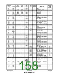
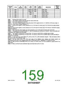
SMBus2
REG
OFFSET
Vbat
POR
OFFSET
(hex)
PCI
RESET
VCC
POR
VTR
POR
SOFT
RESET
TYPE
REGISTER
PM1_EN1
7A
7B
7C
7D
7E
7F
R/W
R/W
R/W
R/W
R/W
R/W
-
-
-
-
-
-
-
-
(Note 7)
0x00
0x00
-
-
-
-
-
-
-
-
-
-
-
-
-
(Note 7)
PM1_EN2
0x00
GPE1_STS 1
GPE1_STS 2
GPE1_EN 1
GPE1_EN 2
-
-
-
0x00
-
-
-
0x00
0x00
Note:
Reserved bits return 0 on read.
Note 1: This register contains some bits that are read or write only.
Note 2: Bit 0 is not cleared by PCI RESET.
Note 3: The Device Disable Register is read-only when GP43 register bit [3:2] = 01 AND the GP43 pin is high, or
when bit 1 of the Device Disable Register is ‘1’.
Note 4: Bit [3] of this register is reset (cleared) on VCC POR and PCI Reset (and VTR POR) for fan output default
at power-up.
Note 4a: Bit [3] of this register is reset (cleared) on VCC POR and PCI Reset (and VTR POR) for TXD2/IRTX output
default at power-up.
Note 5: Bits [3:2] of the GP43 register are reset (cleared) on VCC POR and PCI Reset (and VTR POR).
Note 6: The parallel port interrupt defaults to 1 when the parallel port activate bit is cleared. When the parallel port
is activated, PINT follows the nACK input.
Note 7: This register is powered by VTR and Vbat. It is reset on Vbat POR to a default value of 0x00
Note 7a: This register is powered by VTR and Vbat. It is reset on Vbat POR to a default value of 0x00 and Bit[7] is
cleared on a VTR POR
Note 8: A soft reset only resets Bit[0] (LPC_REQ) of the LPC_ARB Arbitration Register. Bit[1] will always reflect
the current state of the arbitration logic.
Note 9: The two LSBs of the VTR POR reset value of the SMBus2 slave address and enable register are
determined by the state of the strapping option pins, SADR0 and SADR1, following a VTR power-on-reset.
Note 10: Bits[7:0] may be individually reset on Vcc Reset, PCI Reset, and VTR POR if enabled in Logical Device A at
offset 0xF6.
Note 11: Bit[1] is set/reset by the arbitration logic and Read only by the LPC Bus.
SMSC LPC47S45x
Page 159 of 259
Rev. 06-01-06
DATASHEET

 SMSC [ SMSC CORPORATION ]