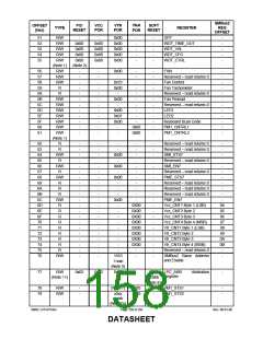
7.5.2 ACPI SUPPORT REGISTER FOR SMI GENERATION
In addition to the SMI, status and enable, registers, the LPC47S45x has implemented the ACPI PM1 and GPE
registers. These registers can be used to generate an SMI event.
To generate an SMI event from the PM1/GPE registers:
Enable Bit[7] EN_SMI of the SMI_EN2 register at offset 17h
Do not enable Bit[0] SCI_EN in the PM1_CNTRL1 register at offset 60h.
Set Bit[6] SMI_SCI_ENB to ‘0’ in the PS_CNTRL register, Logical Device A at offset 0xF8. This bit is used to
generate an SMI for Enabled SCI event
Enable selected SCI events in the PM1 and GPE enable registers.
The ACPI PM1 Control register is implemented in the LPC47S45x to allow the generation of an SMI when the
SLP_EN bit (PM1_CNTRL2 bit 5) is written to ‘1’. The SLP_TYPx field (bits[4:2]) is also read/write and is used to
define the type of hardware sleep state the system enters when the SLP_EN bit is set to one..
The PM1_CNTRL1 and PM1_CNTRL2 registers implement the ACPI PM1 Control register. These registers are
located at the address programmed in the Base I/O address in Logical Device A at the offset of 0x60, 0x61. Software
will treat these as a 16-bit register since the two 8-bit registers are adjacent.
See the Runtime Registers section for description on these registers.
SMSC LPC47S45x
Page 155 of 259
Rev. 06-01-06
DATASHEET

 SMSC [ SMSC CORPORATION ]