6.16 Device Disable Register
There are two Device Disable Registers located in the LPC47S45x.
1. Device Disable Register located in the Runtime Register block at offset 0x22 (accessible by LPC interface only)
2. SMBus2 Device Disable Register located in the SMBus2 Registers at offset 01h (accessible by SMBus2 only)
6.16.1 DEVICE DISABLE REGISTER (LPC ONLY)
The Device Disable Register is located in the PME register block at offset 0x22 from the Runtime Registers Block
base I/O address in logical device A. Bits [3:7] are used to enable/disable the Floppy, Serial Ports, and/or Parallel
Port and Bit[0] is used for Floppy Write Protect. As a security feature, this register’s contents may be locked (i.e.,
Read-Only) by setting Bit[1] Register Lock bit high, which is only cleared on a VCC POR or a PCI Reset. Writes to
this register may also be blocked when the GP43 pin is configured for the Device Disable Register Control function
(GP43 configuration register bit 2 =1) and the GP43 pin is high.
The control register for device disable register is defined in the “Runtime Registers” section and described below.
GPIO Device Disable Register Control
The GPIO pin GP43 is used for the Device Disable Register Control (DDRC) function. Setting bits[3:2] of the GP43
configuration register to ‘01’, selects the DDRC function for the GP43 pin. When bits[3:2]=01 the GP43 pin is an
input, with non-inverted polarity. Bits[3:2] cannot be cleared by writing to these bits; they are cleared by VTR POR,
VCC POR and PCI Reset. That is, when the DDRC function is selected for this pin, it cannot be changed, except by a
VCC POR, PCI Reset or VTR POR. When Register Lock bit in the Device Disable is set to high regardless of the value
of GP43 pin, all the bits in the Device Disable Register are Read Only until a VCC POR.
When the DDRC function is selected for GP43, the Device Disable register is controlled by the value of the GP43 pin
as follows:
If the GP43 pin is high, the Device Disable Register at offset 22h is Read-Only.
If the GP43 pin is low, the Device Disable Register at offset 22h is Read/Write.
The Device Disable register has a Register Lock bit (bit 1) that is cleared on VTR POR, VCC POR and PCI Reset. It
cannot be cleared by software writing to the bit. The Device Disable register is controlled by the Register Lock bit as
follows:
If the Register Lock bit is high, the Device Disable Register is Read-Only,
If the Register Lock bit is low, the Device Disable Register has no effect (default)
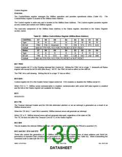
The following table shows two different means of making the DDRC register read only.
DDRC ENABLE
(BIT 2 OF GP43 REG)
DDRC PIN
REGISTER LOCK BIT
REGISTER STATE
X
0
1
1
X
X
0
1
0
0
0
Read Only
Read/Write
Read/Write
Read Only
1
6.16.2 SMBUS2 DEVICE DISABLE REGISTER (SMBUS2 ONLY)
This device disable register is located in the SMBus2 register block and is only accessible through the SMBus2. The
functionality of this register is identical to the LPC device disable register, with the exception to the GP43 pin when it
is configured for it’s DDRC function. Asserting the DDRC function on the GP43 pin has no effect on the SMBus2
Device Disable Register. See SMBus2 Device Disable Control on page 140 for a more detailed description of this
register.
Note: Either device disable register is capable of disabling the Parallel Port, Serial Port 1, Serial Port 2, and the
Floppy by setting the respective bits to ‘1’. For a device to be enabled, both device disable registers must be set the
respective device bit to enabled. Once the register lock bit is set in either register the only way to reset a device
disable bit to enabled is by a VCC POR or a PCI Reset.
Note: The Register Lock bit in each device disable register only effects the register it is located in. (i.e. If the LPC
Device Disable Register is Read-only, the SMBus2 register may be Read/Write). Asserting the DDRC function on
GP43 pin only effects the LPC Device Disable Register.
SMSC LPC47S45x
Page 128 of 259
Rev. 06-01-06
DATASHEET

 SMSC [ SMSC CORPORATION ]